


 Flexible Thinking: PCB Designers Still Wanted
 Connect the Dots: Five Best Practices for Designing Flex and Rigid-flex PCBs
 Tim’s Takeaways: Human Ingenuity and the Rigid-flex PCB
AT&S Starts Construction of First High-tech Manufacturing Facility in Southeast Asia
October 29, 2021 | AT&SEstimated reading time: 2 minutes
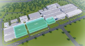
AT&S, one of the globally leading manufacturers of high-end printed circuit boards and IC substrates, headquartered in Austria (Europe), announced detailed project information on the company’s planned investment in a state-of-the-art factory for IC substrates at the Kulim Hi-Tech Park, Kedah.
During a press conference, AT&S CEO Andreas Gerstenmayer and AT&S COO Ingolf Schroeder gave insights into the planned investment, the project scope, technology details, as well as the planned activities to hire approx. 6,000 highly qualified employees.
AT&S’ new campus for the production of IC substrates in Kulim Hi-Tech Park, Kedah, involves a proposed total investment for phase 1 of RM 8.5 billion (€1.7 billion). The construction of the facility is going to start with an official groundbreaking ceremony on October 30, 2021, with commercial operations targeted to come on stream in 2024.
“I want to thank the Malaysian government as well as the MIDA (the government’s principal promotion agency under the Ministry of International Trade and Industry) for the great support throughout the entire process, from the start of our location scouting until today,” says AT&S CEO Andreas Gerstenmayer. “Already today, Malaysia is an important hub for the chip supply chain. We are convinced that Malaysia can further strengthen its position as a technology country and will develop its position in the region as a high-tech manufacturing hub in Asia,” Gerstenmayer says.
Not only will thousands of new jobs be created in the region, but Malaysia will make a name for itself as a hotspot for a completely new, first-of-its-kind technology segment. “AT&S brings the latest generation of high-end technologies to Malaysia and will establish a completely new technology sector in one of the future global microelectronic hotspots. In addition to manufacturing high-tech products, extensive R&D activities will also be conducted at this new site,” AT&S COO Ingolf Schroeder says.
All these activities require a high amount of highly qualified human resources and will boost the region’s labor market. The search profiles for employees at the new AT&S plant range from specialists, managers, and leaders in the areas of electronic, mechanical, and chemical engineers, and business. At the same time, AT&S is also looking for about 4,500 blue-collar workers who can work in a highly sophisticated shop floor environment.
Besides manufacturing, R&D will also be a focus at the new AT&S facility in Kulim. Therefore, AT&S is investigating cooperation and partnerships with leading universities in Malaysia. “These partnerships will not only help us to discover new paths for the microelectronics industry,” Andreas Gerstenmayer says. “They will also make an important contribution to the development of extensive know-how in the various areas of the microelectronics industry for Malaysia and, at the end of the day, contribute to the positive development of the society.”
Share on:


Suggested Items
I-Connect007 Editor’s Choice: Five Must-Reads for the Week
05/03/2024 | Nolan Johnson, I-Connect007This week’s most important news is strategic—and telling. When one puts together the IPC industry reports, we simply have to include the recent conversation with Shawn DuBravac and Tom Kastner. On the design side, check out the latest “On The Line With…” podcast featuring Brad Griffin from Cadence Design Systems, discussing SI and PI in the realm of intelligent system design.
HQ NextPCB of HQ Electronics Debut on the International Stage for Electronics Manufacture at IPC APEX 2024
05/01/2024 | PRNewswireHQ NextPCB of HQ Electronics, a leading Chinese-based multilayer PCB manufacturer and assembly house showcased its industrial prowess on the international stage for the first time at the IPC APEX Expo 2024.
IPC's Vision for Empowering PCB Design Engineers
04/30/2024 | Robert Erickson, IPCAs architects of innovation, printed circuit board designers are tasked with translating increasingly complex concepts into tangible designs that power our modern world. IPC provides the necessary community, standards framework, and education to prepare these pioneers as they explore the boundaries of what’s possible, equipping engineers with the knowledge, skills, and resources required to thrive in an increasingly dynamic field.
On the Line With… Talks With Cadence Expert on SI/PI for PCB Designers
05/02/2024 | I-Connect007In “PCB 3.0: A New Design Methodology—SI/PI for PCB Designers,” subject matter expert Brad Griffin, Cadence Design Systems, discusses how an intelligent system design methodology can move some signal and power integrity decision-making into the physical design space, offering real-time feedback.
USPAE to Springboard U.S. Technology Forward
04/30/2024 | Marcy LaRont, PCB007 MagazineThe U.S. Partnership for Assured Electronics (USPAE) was launched as a nonprofit subsidiary of IPC in 2020, specifically to manage the DoD relationship and access to funding, and to develop a cooperative facility to develop UHDI capabilities in the U.S., not only for the defense sector, but for the whole of the U.S. electronics industry. It is a tall order, but industry veteran Joe O'Neil believes it will happen. Having been tasked with making the UHDI Capable Cooperative Production Facility (UCCPF) a reality, he provides an update on this important project for U.S. electronics manufacturing.