


 The Chemical Connection: Reducing Etch System Water Usage, Part 2
 It’s Only Common Sense: Nice Guys Really Can Finish First
 The Right Approach: I Hear the Train A Comin'
Imec’s Nanomesh Electrodes in Pole Position for High-throughput Electrochemical Applications
December 28, 2022 | ImecEstimated reading time: 2 minutes
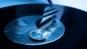
Imec, together with its partner KU Leuven in EnergyVille, announces an important proof point towards implementation of nanomesh structures in high-throughput industrial processes for energy-related applications such as electrolysers, fuel cells and batteries. The researchers have developed a 3D structure made of interconnected nanowires, which can now be used as a freestanding electrode in electrochemical flow cells. The results, published in Materials Today Energy, confirm that the use of these structures can yield a 100-fold increase in current density compared to conventional planar nickel electrodes.
Large-scale production of green hydrogen and green hydrocarbons becomes essential to decarbonize industries. Today, two commercially available options exist for megawatt-scale hydrogen production: classical alkaline water electrolysis (AWE) and proton exchange membrane electrolysis (PEM). However, both technologies face challenges that need to be overcome to further improve the competitiveness of large-scale production of green hydrogen.
Researchers from imec and KU Leuven developed a 3D structure of interconnected nanowires. These nanomesh structures combine high porosity with an extremely high surface area, providing plenty of reaction sites. Due to its unique material properties, nanomesh structures are attractive for numerous electrochemical applications, including electrolysis. They can be created via electroplating, an up-scalable fabrication flow, which makes them cheaper than currently used metal foams.
Until now, non-porous support substrates were needed to provide sufficient mechanical robustness to the highly porous nanomesh. However, to exploit these compelling nano-architectures as freestanding electrodes in electrochemical flow cells, it is essential that the gaseous reagents and products can freely flow in and out. Therefore, the nanowire networks must be supported by a porous structure that is accessible from all sides.
Researchers from imec now published their results on a monolithically integrated nickel nanomesh with an open support grid. This improved nanomesh structure allows gaseous reagents and products to be introduced and removed efficiently from the reaction sites. In an experimental setup they demonstrated that the theoretically available surface area of the nanomesh is almost completely available; resulting in a 100-fold current density increase compared to using conventional planar nickel electrodes. The results confirm that the 3.5 micrometer thin nanomesh electrode has incredible potential in throughput and conversion rates.
"To achieve large-scale production of green hydrogen at offshore wind farms, where space is limited, we need to develop compact electrolysers with high efficiency," said Bart Onsia, business development manager at imec. "These results are a promising step towards the development of new electrolysers components, and we are committed to continuing our research in this area to drive the transition to a more sustainable future."
Philippe Vereecken, imec fellow and part-time professor at KU Leuven: “I am excited that we have been able to further enhance our nanomesh materials and demonstrate their potential in an industry-relevant setup. We have chosen nickel for the current demonstrations for hydrogen production, an area in which we partner with VITO within Hyve, a Belgian consortium that pursues cost-efficient and sustainable hydrogen production on gigawatt scale."
“And the versatility of the nanomesh allows for a much wider portfolio of materials and applications. For instance, we can use copper or silver for CO2 reduction in gas diffusion electrodes," adds Nina Planckensteiner, Marie-Curie post-doctoral researcher at imec. “We are excited to continue exploring the potential of the nanomesh for a wide range of electrochemical applications.”
Share on:


Suggested Items
The Chemical Connection: Reducing Etch System Water Usage, Part 2
05/02/2024 | Don Ball -- Column: The Chemical ConnectionIn my last column, I reviewed some relatively simple ways to reduce water usage in existing etch systems: cutting down cooling coil water flow, adding chillers to replace plant water for cooling, lowering flow rate nozzles for rinses, etc. This month, I’ll continue with more ways to control water usage in your etcher. Most of these are not easily retrofittable to existing equipment but should be given serious consideration when new equipment is contemplated. With the right combination of add-ons, it is possible to bring the amount of water used in an etch system to almost zero.
Designer’s Notebook: What Designers Need to Know About Manufacturing, Part 2
04/24/2024 | Vern Solberg -- Column: Designer's NotebookThe printed circuit board (PCB) is the primary base element for providing the interconnect platform for mounting and electrically joining electronic components. When assessing PCB design complexity, first consider the component area and board area ratio. If the surface area for the component interface is restricted, it may justify adopting multilayer or multilayer sequential buildup (SBU) PCB fabrication to enable a more efficient sub-surface circuit interconnect.
Insulectro’s 'Storekeepers' Extend Their Welcome to Technology Village at IPC APEX EXPO
04/03/2024 | InsulectroInsulectro, the largest distributor of materials for use in the manufacture of PCBs and printed electronics, welcomes attendees to its TECHNOLOGY VILLAGE during this year’s IPC APEX EXPO at the Anaheim Convention Center, April 9-11, 2024.
ENNOVI Introduces a New Flexible Circuit Production Process for Low Voltage Connectivity in EV Battery Cell Contacting Systems
04/03/2024 | PRNewswireENNOVI, a mobility electrification solutions partner, introduces a more advanced and sustainable way of producing flexible circuits for low voltage signals in electric vehicle (EV) battery cell contacting systems.
Heavy Copper PCBs: Bridging the Gap Between Design and Fabrication, Part 1
04/01/2024 | Yash Sutariya, Saturn Electronics ServicesThey call me Sparky. This is due to my talent for getting shocked by a variety of voltages and because I cannot seem to keep my hands out of power control cabinets. While I do not have the time to throw the knife switch to the off position, that doesn’t stop me from sticking screwdrivers into the fuse boxes. In all honesty, I’m lucky to be alive. Fortunately, I also have a talent for building high-voltage heavy copper circuit boards. Since this is where I spend most of my time, I can guide you through some potential design for manufacturability (DFM) hazards you may encounter with heavy copper design.