


 Marcy's Musings: The Growing Industry
 It’s Only Common Sense: Here’s What To Do After IPC APEX EXPO 2024
 Dan’s Biz Bookshelf: Seeing the How
Quantum Light Sources Pave the Way for Optical Circuits
August 1, 2019 | Technical University of MunichEstimated reading time: 2 minutes
An international team headed up by Alexander Holleitner and Jonathan Finley, physicists at the Technical University of Munich (TUM), has succeeded in placing light sources in atomically thin material layers with an accuracy of just a few nanometers. The new method allows for a multitude of applications in quantum technologies, from quantum sensors and transistors in smartphones through to new encryption technologies for data transmission.
Previous circuits on chips rely on electrons as the information carriers. In the future, photons which transmit information at the speed of light will be able to take on this task in optical circuits. Quantum light sources, which are then connected with quantum fiber optic cables and detectors are needed as basic building blocks for such new chips.
An international team headed up by TUM physicists Alexander Holleitner and Jonathan Finley has now succeeded in creating such quantum light sources in atomically thin material layers and placing them with nanometer accuracy.
First Step Towards Optical Quantum Computers
“This constitutes a first key step towards optical quantum computers,” says Julian Klein, lead author of the study. “Because for future applications the light sources must be coupled with photon circuits, waveguides for example, in order to make light-based quantum calculations possible.”
The critical point here is the exact and precisely controllable placement of the light sources. It is possible to create quantum light sources in conventional three-dimensional materials such as diamond or silicon, but they cannot be precisely placed in these materials.
Deterministic Defects
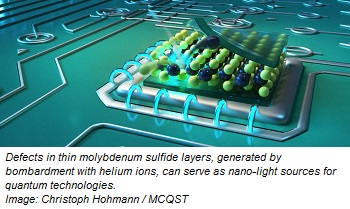
The physicists then used a layer of the semiconductor molybdenum disulfide (MoS2) as the starting material, just three atoms thick. They irradiated this with a helium ion beam which they focused on a surface area of less than one nanometer.
In order to generate optically active defects, the desired quantum light sources, molybdenum or sulfur atoms are precisely hammered out of the layer. The imperfections are traps for so-called excitons, electron-hole pairs, which then emit the desired photons.
Technically, the new helium ion microscope at the Walter Schottky Institute’s Center for Nanotechnology and Nanomaterials, which can be used to irradiate such material with an unparalleled lateral resolution, was of central importance for this.
On The Road to New Light Sources
Together with theorists at TUM, the Max Planck Society, and the University of Bremen, the team developed a model which also describes the energy states observed at the imperfections in theory.
In the future, the researchers also want to create more complex light source patterns, in lateral two-dimensional lattice structures for example, in order to thus also research multi-exciton phenomena or exotic material properties.
This is the experimental gateway to a world which has long only been described in theory within the context of the so-called Bose-Hubbard model which seeks to account for complex processes in solids.
Quantum Sensors, Transistors and Secure Encryption
And there may be progress not only in theory, but also with regard to possible technological developments. Since the light sources always have the same underlying defect in the material, they are theoretically indistinguishable. This allows for applications which are based on the quantum-mechanical principle of entanglement.
“It is possible to integrate our quantum light sources very elegantly into photon circuits,” says Klein. “Owing to the high sensitivity, for example, it is possible to build quantum sensors for smartphones and develop extremely secure encryption technologies for data transmission.”
Share on:


Suggested Items
Three Industry Leaders Receive IPC President’s Award
04/17/2024 | IPCIn recognition of their leadership and significant contributions of time and talent to IPC and the electronics industry, three IPC volunteers were presented with the IPC President’s Award at IPC APEX EXPO in Anaheim, Calif., on April 9, 2024.
FTG Announces Q1 2024 Financial Results
04/12/2024 | Firan Technology Group CorporationDuring Q1 2024, the Corporation has continued to invest in technology in existing sites, grow the business organically, and integrate the two acquisitions completed last year. FTG is strategically deploying its capital in ways that will drive increased shareholder returns for the future in both the near term and long term. Specifically, FTG accomplished the following in Q1 2024, which continues to improve the Corporation and position it for the future:
DuPont Unveils Pyralux ML Laminate Series, Offering High Thermal Management for Extreme Environments
04/09/2024 | DuPontDuPont introduced the DuPont™ Pyralux® ML Series of double-sided metal-clad laminates, a unique addition to its extensive family of Pyralux® laminates for flexible and rigid-flex printed circuit boards (PCBs).
ENNOVI Introduces a New Flexible Circuit Production Process for Low Voltage Connectivity in EV Battery Cell Contacting Systems
04/03/2024 | PRNewswireENNOVI, a mobility electrification solutions partner, introduces a more advanced and sustainable way of producing flexible circuits for low voltage signals in electric vehicle (EV) battery cell contacting systems.
Sunstone Circuits Enhances PCB Online Quote and Order Offerings
04/01/2024 | ASC SunstoneSunstone Circuits, a division of American Standard Circuits, is continuing efforts to make the PCB buying process as easy and frictionless as possible with enhancements to their online OneQuote order form. New features include online quoting and ordering of controlled impedance, update to display ET charges in the pricing matrix, and Gerber file drag-and-drop capabilities, making quoting PCB prototypes and production more efficient.