


 The Right Approach: I Hear the Train A Comin'
 It’s Only Common Sense: OCCAM—the Time Is Now
 Marcy's Musings: The Growing Industry
A Modified Device Fabrication Process Achieves Enhanced Spin Transport in Graphene
August 5, 2019 | ICN2Estimated reading time: 2 minutes
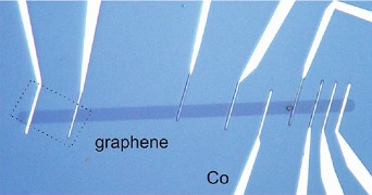
Researchers from the ICN2 Physics and Engineering of Nanodevices Group have proposed a modified graphene-based nanodevice fabrication technique that has increased up to three times the spin lifetime and relaxation length compared to previous work of the same kind. The work was fruit of the collaboration with Imec and K.U. Leuven (Belgium). The results have been published in 2D Materials and are expected to empower investigations on large-scale spintronic applications.
Spintronics is a field of research that was born in the 1980s. It amplifies the potential of traditional electronics by exploiting the electron’s spin degree of freedom, in addition to the usual state of charge. In the end, the goal is the same: to obtain devices to store, process and read information, but with enhanced characteristics such as lower power consumption, less heat dissipation, higher speed, etc. Although spintronics has not yet become as widespread as its conventional predecessor, some current devices are based on this new approach, such as magnetic hard disks, magnetic random access memories and magnetic sensors with varied applications in industrial environments, robotics and automotive industry.
Graphene is a promising material in this field. Spins can flow efficiently in it over long distances, meaning that they do not change their state (let’s say, from “up” to “down”) for a relatively long time. Due to its large-scale production, CVD graphene is becoming popular to fabricate spintronic devices. However, impurities arising from the graphene growth and device fabrication process limit its performance.
A team of scientists from the ICN2 Physics and Engineering of Nanodevices Group, led by ICREA Prof. Sergio O. Valenzuela, has proposed a high-yield device fabrication process from CVD graphene that has improved substantially its spin parameters. The work, whose first author is Zewdu M. Gebeyehu, was fruit of a collaboration with Imec and K.U. Leuven (Belgium). The results have been published in 2D Materials.
They demonstrate a spin signal measured across a 30 µm long channel with room-temperature spin lifetimes of up to 3 ns and spin relaxation lengths of up to 9 µm in monolayer graphene on SiO2/Si substrates. These spin parameters are the highest values for any form of graphene (both exfoliated and CVD graphene) on a standard SiO2/Si substrate.
To achieve this enhanced spin performance, the researchers used CVD graphene grown on a platinum foil and they modified the device fabrication technique so as to reduce the impurity levels associated with the graphene growth and fabrication steps. The latter requires the optimization of several standard processes, involving the preselection of high-quality uniform graphene with low level of impurities, an etching step combining e-beam lithography and oxygen plasma and a suitable post-annealing in high vacuum. The approach can be scaled and allows a highly reproducible fabrication of devices, which is the main requirement for potential industrialization.
The improvement on the spin parameters together with the reproducibility of the device fabrication process brings us closer to the realization of complex circuit architectures for spintronic devices such as spin logic and logic-in-memory for beyond CMOS computing.
Share on:


Suggested Items
Koh Young Showcases Award-winning Inspection Solutions at SMTconnect with SmartRep in Hall 4A.225
04/25/2024 | Koh Young TechnologyKoh Young Technology, the industry leader in True 3D measurement-based inspection solutions, will showcase an array of award-winning inspection and measurement solutions at SMTconnect alongside its sales partner, SmartRep, in booth 4A.225 at NürnbergMesse from June 11-13, 2023. The following offers a glimpse into what Koh Young will present at the tradeshow:
Real Time with… IPC APEX EXPO 2024: Plasmatreat: Innovative Surface Preparation Solutions
04/25/2024 | Real Time with...IPC APEX EXPOIn this interview, Editor Nolan Johnson speaks with Hardev Grewal, CEO and president of Plasmatreat, a developer of atmospheric plasma solutions. Plasmatreat uses clean compressed air and electricity to create plasma, offering environmentally friendly methods for surface preparation. Their technology measures plasma density for process optimization and can remove organic micro-contamination. Nolan and Hardev also discuss REDOX-Tool, a new technology for removing metal oxides.
KYZEN to Promote Pair of Stencil Cleaning Chemistries at SMTA Ciudad Jaurez Expo & Tech Forum
04/25/2024 | KYZEN'KYZEN, the global leader in innovative environmentally friendly cleaning chemistries, will exhibit at the SMTA Ciudad Juarez Expo & Tech Forum, scheduled to take place Thursday, May 9, 2024 at the Injectronic Convention Center in Ciudad Jaurez, Chihuahua, Mexico. During the event the KYZEN Clean Team will focus on understencil cleaning products KYZEN E5631J and CYBERSOLV C8882.
Cadence, TSMC Collaborate on Wide-Ranging Innovations to Transform System and Semiconductor Design
04/25/2024 | Cadence Design SystemsCadence Design Systems, Inc. and TSMC have extended their longstanding collaboration by announcing a broad range of innovative technology advancements to accelerate design, including developments ranging from 3D-IC and advanced process nodes to design IP and photonics.
Listen Up! The Intricacies of PCB Drilling Detailed in New Podcast Episode
04/25/2024 | I-Connect007In episode 5 of the podcast series, On the Line With: Designing for Reality, Nolan Johnson and Matt Stevenson continue down the manufacturing process, this time focusing on the post-lamination drilling process for PCBs. Matt and Nolan delve into the intricacies of the PCB drilling process, highlighting the importance of hole quality, drill parameters, and design optimization to ensure smooth manufacturing. The conversation covers topics such as drill bit sizes, aspect ratios, vias, challenges in drilling, and ways to enhance efficiency in the drilling department.