


 Marcy's Musings: The Growing Industry
 It’s Only Common Sense: Here’s What To Do After IPC APEX EXPO 2024
 Dan’s Biz Bookshelf: Seeing the How
Greener, Faster and Cheaper Way to Make Patterned Metals for Solar Cells and Electronics
August 14, 2019 | University of WarwickEstimated reading time: 2 minutes
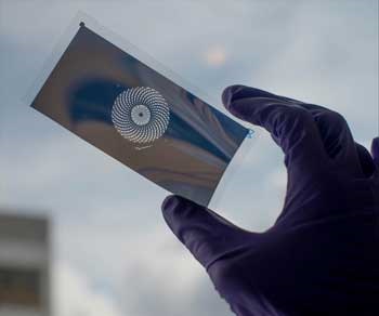
An innovative way to pattern metals has been discovered by scientists in the Department of Chemistry at the University of Warwick, which could make the next generation of solar panels more sustainable and cheaper.
Silver and copper are the most widely used electrical conductors in modern electronics and solar cells. However, conventional methods of patterning these metals to make the desired pattern of conducting lines are based on selectively removing metal from a film by etching using harmful chemicals or printing from costly metal inks.
Scientists from the Department of Chemistry at the University of Warwick, have developed a way of patterning these metals that is likely to prove much more sustainable and cheaper for large scale production, because there is no metal waste or use of toxic chemicals, and the fabrication method is compatible with continuous roll-to-roll processing.
The work is reported in the paper ‘Selective deposition of silver and copper films by condensation coefficient modulation’ published as an advanced article in the journal Materials Horizons ("Selective deposition of silver and copper films by condensation coefficient modulation").
Thanks to £1.15 M funding from the UK Engineering and Physical Sciences Research Council, Dr Ross Hatton and Dr Silvia Varagnolo have discovered that silver and copper do not condense onto extremely thin films of certain highly fluorinated organic compounds when the metal is deposited by simple thermal evaporation.
Thermal evaporation is already widely used on a large scale to make the thin metal film on the inside of crisp packets, and organofluorine compounds are already common place as the basis of non-stick cooking pans.
The researchers have shown that the organofluorine layer need only be 10 billionths of a metre thick to be effective, and so only tiny amounts are needed.
This unconventional approach also leaves the metal surface uncontaminated, which Hatton believes will be particularly important for the next generation sensors, which often require uncontaminated patterned films of these metals as platforms onto which sensing molecules can be attached.
To help address the challenges posed by climate change, there is a need for colour tuneable, flexible and light weight solar cells that can be produced at low cost, particularly for applications where conventional rigid silicon solar cells are unsuitable such as in electric cars and semi-transparent solar cells for buildings.
Solar cells based on thin films of organic, perovskite or nano-crystal semiconductors all have potential to meet this need, although they all require a low cost, flexible transparent electrode. Hatton and his team have used their method to fabricate semi-transparent organic solar cells in which the top silver electrode is patterned with millions of tiny apertures per square centimetre, which cannot be achieved by any other scalable means directly on top of an organic electronic device.
Dr Hatton from the Department of Chemistry at the University of Warwick comments: “This innovation enables us to realise the dream of truly flexible, transparent electrodes matched to needs of the emerging generation of thin film solar cells, as well as having numerous other potential applications ranging from sensors to low-emissivity glass.”
Share on:


Suggested Items
Insulectro’s 'Storekeepers' Extend Their Welcome to Technology Village at IPC APEX EXPO
04/03/2024 | InsulectroInsulectro, the largest distributor of materials for use in the manufacture of PCBs and printed electronics, welcomes attendees to its TECHNOLOGY VILLAGE during this year’s IPC APEX EXPO at the Anaheim Convention Center, April 9-11, 2024.
ENNOVI Introduces a New Flexible Circuit Production Process for Low Voltage Connectivity in EV Battery Cell Contacting Systems
04/03/2024 | PRNewswireENNOVI, a mobility electrification solutions partner, introduces a more advanced and sustainable way of producing flexible circuits for low voltage signals in electric vehicle (EV) battery cell contacting systems.
Heavy Copper PCBs: Bridging the Gap Between Design and Fabrication, Part 1
04/01/2024 | Yash Sutariya, Saturn Electronics ServicesThey call me Sparky. This is due to my talent for getting shocked by a variety of voltages and because I cannot seem to keep my hands out of power control cabinets. While I do not have the time to throw the knife switch to the off position, that doesn’t stop me from sticking screwdrivers into the fuse boxes. In all honesty, I’m lucky to be alive. Fortunately, I also have a talent for building high-voltage heavy copper circuit boards. Since this is where I spend most of my time, I can guide you through some potential design for manufacturability (DFM) hazards you may encounter with heavy copper design.
Trouble in Your Tank: Supporting IC Substrates and Advanced Packaging, Part 5
03/19/2024 | Michael Carano -- Column: Trouble in Your TankDirect metallization systems based on conductive graphite or carbon dispersion are quickly gaining acceptance worldwide. Indeed, the environmental and productivity gains one can achieve with these processes are outstanding. In today’s highly competitive and litigious environment, direct metallization reduces costs associated with compliance, waste treatment, and legal issues related to chemical exposure. What makes these processes leaders in the direct metallization space?
AT&S Shines with Purest Copper on World Recycling Day
03/18/2024 | AT&SThe Styrian microelectronics specialist AT&S is taking World Recycling Day as an opportunity to review the progress that has been made in recent months at its sites around the world in terms of the efficient use of resources: