


 It’s Only Common Sense: OCCAM—the Time Is Now
 Marcy's Musings: The Growing Industry
 Dan’s Biz Bookshelf: Seeing the How
Breakthrough Enables Bezelless Notebook and Tablet Display
August 20, 2019 | Cambridge NetworkEstimated reading time: 2 minutes
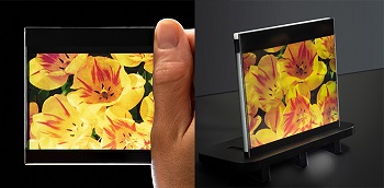
FlexEnable, the leader in the development and industrialisation of flexible organic electronics, has revealed an ultra-narrow border organic LCD (OLCD). By exploiting the truly flexible nature of the organic thin-film transistors (OTFTs) on which OLCD is based, it is now possible to fold the borders behind the display for the first time. This major breakthrough provides a completely new approach to bezel-less screens that cannot be achieved with glass displays.
OLCD, which offers the same quality and performance as traditional glass LCDs, can bring unique benefits to notebooks, tablets, TVs and monitors by responding to the increasing demand for larger displays with smaller to no borders. The bezel size allowed by OLCD is independent of the display size or resolution, and the OLCD technology itself is cost-effectively scalable to large display sizes. Moreover, OLCD can make a notebook up to 100 grams lighter and 0.5 mm thinner.
Chuck Milligan, CEO of FlexEnable, said, “By exploiting the unique properties of FlexEnable’s organic transistors platform, we have proven that it can also provide a route to borderless displays and thus further expand the applications of thin, light and conformable OLCDs. For example, removing the borders of the display allows a larger screen to fit into the same size notebook. This breakthrough enables us to address a multi-billion display market for notebooks, tablets, monitors and TVs as well as surface-integrated displays for automotive interiors.”
OLCD can be easily curved and shaped to enable new form factors in a wide range of products including consumer electronics, smart home devices, automotive displays and beyond. The technology is being implemented into existing manufacturing lines in Asia and is expected to be in production in 2020.
About FlexEnable
FlexEnable’s award-winning organic electronics platform enables glass-free flexible displays, sensors and optics that can be applied to almost any surface. The company has developed and industrialised a complete low-temperature manufacturing process for small and large-area electronics on ultra-thin plastic substrates. This low cost technology platform is compatible with existing flat panel display production lines utilising most of the established infrastructure and providing an optimal route to manufacture. FlexEnable’s conformable, ultra-thin, ultra-light and shatterproof displays and sensors bring game-changing capabilities to products across consumer electronics, automotive, smart home devices, digital signage and beyond. FlexEnable transfers and licenses its unique technology platform to manufacturing partners, and works directly with OEM and Tier 1 companies on developing next generation product designs. The company is headquartered in Cambridge, UK and its origins lie in the University of Cambridge’s world-famous Cavendish Laboratory. It taps into the world’s leading flexible electronics engineering talent, with collective experience of over 700 engineering years and holding over 650 patents.
Share on:


Suggested Items
Book Excerpt: The Printed Circuit Assembler’s Guide to... Factory Analytics
04/24/2024 | I-Connect007 Editorial TeamIn our fast-changing, deeply competitive, and margin-tight industry, factory analytics can be the key to unlocking untapped improvements to guarantee a thriving business. On top of that, electronics manufacturers are facing a tremendous burden to do more with less. If you don't already have a copy of this book, what follows is an excerpt from the introduction chapter of 'The Printed Circuit Assembler’s Guide to... Factory Analytics: Unlocking Efficiency Through Data Insights' to whet your appetite.
Listen Up! The Intricacies of PCB Drilling Detailed in New Podcast Episode
04/25/2024 | I-Connect007In episode 5 of the podcast series, On the Line With: Designing for Reality, Nolan Johnson and Matt Stevenson continue down the manufacturing process, this time focusing on the post-lamination drilling process for PCBs. Matt and Nolan delve into the intricacies of the PCB drilling process, highlighting the importance of hole quality, drill parameters, and design optimization to ensure smooth manufacturing. The conversation covers topics such as drill bit sizes, aspect ratios, vias, challenges in drilling, and ways to enhance efficiency in the drilling department.
Elevating PCB Design Engineering With IPC Programs
04/24/2024 | Cory Blaylock, IPCIn a monumental stride for the electronics manufacturing industry, IPC has successfully championed the recognition of the PCB Design Engineer as an official occupation by the U.S. Department of Labor (DOL). This pivotal achievement not only underscores the critical role of PCB design engineers within the technology landscape, but also marks the beginning of a transformative journey toward nurturing a robust, skilled workforce ready to propel our industry into the future.
Winner of The Science Show Rakett 69 Receives Incap Scholarship
04/24/2024 | IncapThe winner of the Rakett 69 science show, Andri Türkson, who stood out as an electronics enthusiast, received a scholarship from Incap Estonia, along with an internship opportunity in Saaremaa.
Alternative Manufacturing Inc. Awarded QML Requalification to IPC J-STD-001 and IPC-A-610
04/24/2024 | IPCIPC's Validation Services Program has awarded an IPC J-STD-001 and IPC-A-610 Qualified Manufacturers Listing (QML) requalification to Alternative Manufacturing Inc (AMI).