


 The Right Approach: I Hear the Train A Comin'
 It’s Only Common Sense: OCCAM—the Time Is Now
 Marcy's Musings: The Growing Industry
Creating New Opportunities From Nanoscale Materials
September 9, 2019 | MITEstimated reading time: 12 minutes
A hundred years ago, “2d” meant a two-penny, or 1-inch, nail. Today, “2-D” encompasses a broad range of atomically thin flat materials, many with exotic properties not found in the bulk equivalents of the same materials, with graphene — the single-atom-thick form of carbon — perhaps the most prominent. While many researchers at MIT and elsewhere are exploring two-dimensional materials and their special properties, Frances M. Ross, the Ellen Swallow Richards Professor in Materials Science and Engineering, is interested in what happens when these 2-D materials and ordinary 3-D materials come together.
“We’re interested in the interface between a 2-D material and a 3-D material because every 2-D material that you want to use in an application, such as an electronic device, still has to talk to the outside world, which is three-dimensional,” Ross says.
“We’re at an interesting time because there are immense developments in instrumentation for electron microscopy, and there is great interest in materials with very precisely controlled structures and properties, and these two things cross in a fascinating way,” says Ross.
“The opportunities are very exciting,” Ross says. “We’re going to be really improving the characterization capabilities here at MIT.” Ross specializes in examining how nanoscale materials grow and react in both gases and liquid media, by recording movies using electron microscopy. Microscopy of reactions in liquids is particularly useful for understanding the mechanisms of electrochemical reactions that govern the performance of catalysts, batteries, fuel cells, and other important technologies. “In the case of liquid phase microscopy, you can also look at corrosion where things dissolve away, while in gases you can look at how individual crystals grow or how materials react with, say, oxygen,” she says.
Ross joined the Department of Materials Science and Engineering (DMSE) faculty last year, moving from the nanoscale materials analysis department at the IBM Thomas J. Watson Research Center. “I learned a tremendous amount from my IBM colleagues and hope to extend our research in material design and growth in new directions,” she says.
Recording Movies
During a recent visit to her lab, Ross explained an experimental setup donated to MIT by IBM. An ultra-high vacuum evaporator system arrived first, to be attached later directly onto a specially designed transmission electron microscope. “This gives powerful possibilities,” Ross explains. “We can put a sample in the vacuum, clean it, do all sorts of things to it such as heating and adding other materials, then transfer it under vacuum into the microscope, where we can do more experiments while we record images. So we can, for example, deposit silicon or germanium, or evaporate metals, while the sample is in the microscope and the electron beam is shining through it, and we are recording a movie of the process.”
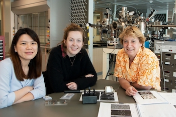
While waiting this spring for the transmission electron microscope to be set up, members of Ross’ seven-member research group, including materials science and engineering postdoc Shu Fen Tan and graduate student Kate Reidy, made and studied a variety of self-assembled structures. The evaporator system was housed temporarily on the fifth-level prototyping space of MIT.nano while Ross’s lab was being readied in Building 13. “MIT.nano had the resources and space; we were happy to be able to help,” says Anna Osherov, MIT.nano assistant director of user services.
“All of us are interested in this grand challenge of materials science, which is: ‘How do you make a material with the properties you want and, in particular, how do you use nanoscale dimensions to tweak the properties, and create new properties, that you can’t get from bulk materials?’” Ross says.
Using the ultra-high vacuum system, graduate student Kate Reidy formed structures of gold and niobium on several 2-D materials. “Gold loves to grow into little triangles,” Ross notes. “We’ve been talking to people in physics and materials science about which combinations of materials are the most important to them in terms of controlling the structures and the interfaces between the components in order to give some improvement in the properties of the material,” she notes.
Shu Fen Tan synthesized nickel-platinum nanoparticles and examined them using another technique, liquid cell electron microscopy. She could arrange for only the nickel to dissolve, leaving behind spiky skeletons of platinum. “Inside the liquid cell, we are able to see this whole process at high spatial and temporal resolutions,” Tan says. She explains that platinum is a noble metal and less reactive than nickel, so under the right conditions the nickel participates in an electrochemical dissolution reaction and the platinum is left behind.
Platinum is a well-known catalyst in organic chemistry and fuel cell materials, Tan notes, but it is also expensive, so finding combinations with less-expensive materials such as nickel is desirable.
“This is an example of the range of materials reactions you can image in the electron microscope using the liquid cell technique,” Ross says. “You can grow materials; you can etch them away; you can look at, for example, bubble formation and fluid motion.”
A particularly important application of this technique is to study cycling of battery materials. “Obviously, I can’t put an AA battery in here, but you could set up the important materials inside this very small liquid cell and then you can cycle it back and forth and ask, if I charge and discharge it 10 times, what happens? It does not work just as well as before — how does it fail?” Ross asks. “Some kind of failure analysis and all the intermediate stages of charging and discharging can be observed in the liquid cell.
“Microscopy experiments where you see every step of a reaction give you a much better chance of understanding what’s going on,” Ross says.
Page 1 of 3
Share on:


Suggested Items
Real Time with... IPC APEX EXPO 2024: Sustainability in the Industry
04/26/2024 | Real Time with...IPC APEX EXPOGuest Editor Henry Crandall and Chris Nash of Indium Corporation discuss the company's 90th anniversary and its focus on sustainability. They focus on the benefits of sustainable materials, their compatibility, and value propositions. The conversation also highlights how Durafuse LT technology's role in reducing reflow temperatures is leading to significant cost and energy savings. Nash also touches on downstream sustainability efforts such as using recycled materials for packaging.
SMC Korea 2024 to Highlight Semiconductor Materials Trends and Innovations on Industry’s Path to $1 Trillion
04/24/2024 | SEMIWith Korea a major consumer of semiconductor materials and advanced materials a key driver of innovation on the industry’s path to $1 trillion, industry leaders and experts will gather at SMC (Strategic Materials Conference) Korea 2024 on May 29 at the Suwon Convention Center in Gyeonggi-do, South Korea to provide insights into the latest materials developments and trends. Registration is open.
Groundbreaking Ceremony Marks the Beginning of a New Era for Newccess Industrial; The Construction of the MINGXIN Building
04/12/2024 | Newccess IndustrialOn a clear and sunny day in March, the groundbreaking ceremony for the MINGXIN Building took place in Shenzhen, China. This moment marked the official commencement of construction for a project that will reshape the semiconductor materials industry.
The Need for a Holistic Global Sustainability Standard
04/10/2024 | Michael Ford, Aegis SoftwareNo one can deny that the resources of our fragile planet are finite. The environment seems like a third party, subject to constant degradation. We’re acutely aware of the effects of pollution on our climate, and despite our “throw-away” culture, recycling and recovery of materials has remained relatively expensive, even as we use more energy just to survive.
iNEMI Publishes Four Roadmap Topics
04/04/2024 | iNEMIThe International Electronics Manufacturing Initiative (iNEMI) announces the availability of the first roadmap topics in the new iNEMI Roadmap format. Printed circuit boards, sustainable electronics, smart manufacturing, and mmWave materials and test are now available online.