


 It’s Only Common Sense: OCCAM—the Time Is Now
 Marcy's Musings: The Growing Industry
 Dan’s Biz Bookshelf: Seeing the How
Getting a Look Under the Hood of Topological Insulators
September 11, 2019 | Argonne National LaboratoryEstimated reading time: 2 minutes
Certain materials, like copper, conduct electricity very well. Other materials, like glass, do not. A certain kind of material, called a topological insulator, acts partially like one and partially like the other ― it behaves like a conductor at its surface and an insulator in its interior.
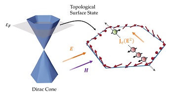
Image Caption: The specific relation between electronic states in a topological insulator and momentum leads to an asymmetric accumulation of spin, depicted on the right, which gives rise to an electric current to second order in an applied electric field E. (Image by Shulei Zhang / Argonne National Laboratory.)
Because of topological insulators’ unique electronic properties and their potential use in spintronic devices and even conceivably as transistors for quantum computers, scientists at the U.S. Department of Energy’s (DOE) Argonne National Laboratory are interested in investigating the special relationship between two properties of the conducting surface electrons in these materials.
In topological insulators, the spin and momentum of each surface electrons are so closely tied that, in scientific parlance, they are locked to one another. “Spin-momentum locking is like having a basketball that must rotate in a specific direction depending on its trajectory down the court,” said Argonne materials scientist Olle Heinonen. “Because an electron also carries a magnetic moment, you can use spin-momentum locking to manipulate magnetic systems very efficiently.”
The electronic structure of topological insulators, including the specifics of spin-momentum locking, may be reflected in the transport behavior of electrons in the materials. To explore the novel behavior of electrons in the topological materials, Argonne scientists worked with scientists at the National University of Singapore, who performed a transport experiment that provided a new perspective of the topologically protected electronic structure.
Heinonen and former Argonne postdoctoral researcher Shulei Zhang described how in the transport experiment a magnetic field applied in the plane of a thin film of a topological insulator can create a voltage in the direction perpendicular to the applied electric current — a phenomenon called a nonlinear planar Hall effect. By varying the direction and intensity of the magnetic field, the Argonne researchers and their colleagues could ascertain from the resulting resistance information as to how the electrons are distributed in terms of their momenta and spin.
“If you know how magnetic fields applied in different directions would affect the nonlinear Hall current measured, you can use our theoretical model to map out how the electrons’ momenta and spins are distributed,” Zhang said. “Then, because of the way we can see more precisely how the electromagnetic fields interact with the surface conduction electrons, we can get much more detailed information of the surface electronic structure of topological insulators.”
The tie between the nonlinear planar Hall effect and the topological surface states with spin-momentum locking is, according to Heinonen, a “macroscopic-microscopic relationship.” “It really gives us a look under the hood,” he said.
A paper based on the study, “Nonlinear planar hall effect,” appeared in the July 1 online edition of Physical Review Letters.
Researchers from the University of Missouri also collaborated on the work. Funding for the study came from DOE’s Office of Science (Office of Basic Energy Sciences).
Share on:


Suggested Items
Designer’s Notebook: What Designers Need to Know About Manufacturing, Part 2
04/24/2024 | Vern Solberg -- Column: Designer's NotebookThe printed circuit board (PCB) is the primary base element for providing the interconnect platform for mounting and electrically joining electronic components. When assessing PCB design complexity, first consider the component area and board area ratio. If the surface area for the component interface is restricted, it may justify adopting multilayer or multilayer sequential buildup (SBU) PCB fabrication to enable a more efficient sub-surface circuit interconnect.
Insulectro’s 'Storekeepers' Extend Their Welcome to Technology Village at IPC APEX EXPO
04/03/2024 | InsulectroInsulectro, the largest distributor of materials for use in the manufacture of PCBs and printed electronics, welcomes attendees to its TECHNOLOGY VILLAGE during this year’s IPC APEX EXPO at the Anaheim Convention Center, April 9-11, 2024.
ENNOVI Introduces a New Flexible Circuit Production Process for Low Voltage Connectivity in EV Battery Cell Contacting Systems
04/03/2024 | PRNewswireENNOVI, a mobility electrification solutions partner, introduces a more advanced and sustainable way of producing flexible circuits for low voltage signals in electric vehicle (EV) battery cell contacting systems.
Heavy Copper PCBs: Bridging the Gap Between Design and Fabrication, Part 1
04/01/2024 | Yash Sutariya, Saturn Electronics ServicesThey call me Sparky. This is due to my talent for getting shocked by a variety of voltages and because I cannot seem to keep my hands out of power control cabinets. While I do not have the time to throw the knife switch to the off position, that doesn’t stop me from sticking screwdrivers into the fuse boxes. In all honesty, I’m lucky to be alive. Fortunately, I also have a talent for building high-voltage heavy copper circuit boards. Since this is where I spend most of my time, I can guide you through some potential design for manufacturability (DFM) hazards you may encounter with heavy copper design.
Trouble in Your Tank: Supporting IC Substrates and Advanced Packaging, Part 5
03/19/2024 | Michael Carano -- Column: Trouble in Your TankDirect metallization systems based on conductive graphite or carbon dispersion are quickly gaining acceptance worldwide. Indeed, the environmental and productivity gains one can achieve with these processes are outstanding. In today’s highly competitive and litigious environment, direct metallization reduces costs associated with compliance, waste treatment, and legal issues related to chemical exposure. What makes these processes leaders in the direct metallization space?