


 It’s Only Common Sense: OCCAM—the Time Is Now
 Marcy's Musings: The Growing Industry
 Dan’s Biz Bookshelf: Seeing the How
Samsung Electronics Begins Mass Production At New EUV Manufacturing Line
February 20, 2020 | Business WireEstimated reading time: 1 minute
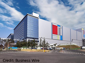
Samsung Electronics Co., Ltd., a world leader in advanced semiconductor technology, today announced that its new cutting-edge semiconductor fabrication line in Hwaseong, Korea, has begun mass production.
The facility, V1, is Samsung’s first semiconductor production line dedicated to the extreme ultraviolet (EUV) lithography technology and produces chips using process node of 7 nanometer (nm) and below. The V1 line broke ground in February 2018, and began test wafer production in the second half of 2019. Its first products will be delivered to customers in the first quarter.
"Along with technology leadership and design infrastructure, manufacturing excellence is one of the most important elements of the foundry business,” said Dr. ES Jung, President and Head of Foundry Business at Samsung Electronics. "As we ramp up production, the V1 line will enhance our ability to respond to market demand and expand opportunities to support our customers."
The V1 line is currently producing state-of-the-art mobile chips with 7 and 6nm process technology and will continue to adopt finer circuitry up to the 3nm process node.
By the end of 2020, the cumulative total investment in the V1 line will reach USD 6 billion in accordance with Samsung’s plan and the total capacity from 7nm and below process node is expected to triple from that of 2019. Together with the S3 line, the V1 line is expected to play a pivotal role in responding to fast-growing global market demand for single-digit node foundry technologies.
As semiconductor geometries grow smaller, the adoption of EUV lithography technology has become increasingly important, as it enables scaling down of complex patterns on wafers and provides an optimal choice for next-generation applications such as 5G, AI, and Automotive.
With the V1 line in operation, Samsung now has a total of six foundry production lines in South Korea and the United States, including five 12-inch lines and one 8-inch line.
Share on:


Suggested Items
Boeing Opens Research & Technology Center in Japan
04/23/2024 | BoeingBoeing today opened a Boeing Research & Technology (BR&T) Center in Japan that will focus on innovation to enable the commercial aviation industry meet its goal of net zero carbon emissions by 2050.
Schweizer Electronic Appoints Thomas Gottwald as New Member of the Executive Board
04/23/2024 | Schweizer Electronic AGThe Supervisory Board of Schweizer Electronic AG has appointed Mr. Thomas Gottwald to the Executive Board as CTO (Chief Technology Officer) for a period of 3 years with effect from 1 May 2024.
US Department of Defense Selects Intel Foundry for Phase Three of RAMP-C
04/23/2024 | IntelThe U.S. Department of Defense (DoD) has awarded Intel Foundry Phase Three of its Rapid Assured Microelectronics Prototypes - Commercial (RAMP-C) program.
Real Time with... IPC APEX EXPO 2024: Industrial Quality Solutions from Zeiss
04/23/2024 | Real Time with...IPC APEX EXPOEditor Nolan Johnson and Herminso Gomez of Zeiss Group discuss the company's industrial quality solutions, with a focus on X-ray technology. Zeiss provides a range of microscopy options and Herminso highlights the advantages of X-ray technology for aerospace, medical, and consumer electronics sectors.
AIM Solder’s Dillon Zhu to Present on Ultraminiature Soldering at SMTA China East
04/22/2024 | AIMAIM Solder, a leading global manufacturer of solder assembly materials for the electronics industry, is pleased to announce that Dillon Zhu will present on the topic: Ultraminiature Soldering: Techniques, Technologies, and Standards at SMTA China East. This event is being held at the Shanghai World Expo Exhibition & Convention Center from April 24-25.