


 Marcy's Musings: The Growing Industry
 It’s Only Common Sense: Here’s What To Do After IPC APEX EXPO 2024
 Dan’s Biz Bookshelf: Seeing the How
Samsung Electronics Expands its Foundry Capacity with A New Production Line in Pyeongtaek, Korea
May 21, 2020 | Business WireEstimated reading time: 1 minute
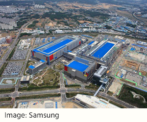
Samsung Electronics Co., Ltd., a world leader in advanced semiconductor technology, today announced plans to boost its foundry capacity at the company's new production line in Pyeongtaek, Korea, to meet growing global demand for cutting-edge extreme ultraviolet (EUV) solutions.
The new foundry line, which will focus on EUV-based 5 nanometer (nm) and below process technology, has just commenced construction this month and is expected to be in full operation in the second half of 2021. It will play a pivotal role as Samsung aims to expand the use of state-of-the-art process technologies across a myriad of current and next generation applications, including 5G, high-performance computing (HPC) and artificial intelligence (AI).
“This new production facility will expand Samsung’s manufacturing capabilities for sub-5nm process and enable us to rapidly respond to the increasing demand for EUV-based solutions,” said Dr. ES Jung, President and Head of Foundry Business at Samsung Electronics. “We remain committed to addressing the needs of our customers through active investments and recruitment of talents. This will enable us to continue to break new ground while driving robust growth for Samsung’s foundry business.”
Following the initial mass production of the EUV-based 7nm process in early 2019, Samsung recently added a new EUV-dedicated V1 line in Hwaseong, Korea, to its global foundry network. With the new Pyeongtaek facility starting full operation in 2021, Samsung’s foundry capacity based on EUV is expected to increase significantly.
Samsung is scheduled to start mass production of 5nm EUV process in the Hwaseong fab in the second half of this year.
With the addition of the Pyeongtaek fab, Samsung will have a total of seven foundry production lines located in South Korea and the United States, comprised of six 12-inch lines and one 8-inch line.
Share on:


Suggested Items
Intel Brings AI-Platform Innovation to Life at the Olympic Games
04/18/2024 | BUSINESS WIREIntel announced its plans for the Olympic and Paralympic Games Paris 2024. Bringing AI Everywhere, Intel will implement artificial intelligence technology powered by Intel processors on the world’s biggest stage.
The Connection Between Wire Harness and Box Build
04/17/2024 | Nolan Johnson, I-Connect007Christina Rutherford is a technical lead and expert in materials engineering at Honeywell, where her specialty is the design, specification, and manufacture of cables and wire harnesses. Rutherford also sits on the committee for IPC/WHMA-A-620. In this conversation, we explore the changing dynamics in wire harnesses and how they relate to box build. Christina’s standards work allows her to draw insightful parallels between wire harness and box build.
Real Time with... IPC APEX EXPO 2024: Innovations in Thermal, Warpage, and Strain Metrology
04/17/2024 | Real Time with...IPC APEX EXPOEditor Nolan Johnson talks with Neil Hubble, president of Akrometrix, about the company's leadership in thermal, warpage, and strain metrology. Neil details how Akrometrix is committed to addressing customer challenges through technological evolution, innovative solutions, and a focus on data processing. A tabletop unit for thermal warpage testing is showcased at IPC APEX EXPO this year.
Hentec/RPS Publishes an Essential Guide to Selective Soldering Processing Tech Paper
04/17/2024 | Hentec Industries/RPS AutomationHentec Industries/RPS Automation, a leading manufacturer of selective soldering, lead tinning and solderability test equipment, announces that it has published a technical paper describing the critical process parameters that need to be optimized to ensure optimal results and guarantee the utmost in end-product quality.
Connect the Dots: Designing for Reality: Prioritizing Manufacturability
04/11/2024 | Matt Stevenson -- Column: Connect the DotsRealistic PCB designs should prioritize manufacturability and reliability of the PCB as well as meet the other design requirements. To do so, one must account for the production variables associated with individual manufacturing partners. Understanding and creating robust PCB designs, especially in terms of board manufacturing, requires a lot of attention to detail. When more detail is included in the design, the manufacturing process goes more smoothly, and process yields are higher.