


 Marcy's Musings: The Growing Industry
 It’s Only Common Sense: Here’s What To Do After IPC APEX EXPO 2024
 Dan’s Biz Bookshelf: Seeing the How
A Different Type of 2D Semiconductor
September 28, 2015 | Lawrence Berkeley National LaboratoryEstimated reading time: 3 minutes
To the growing list of two-dimensional semiconductors, such as graphene, boron nitride, and molybdenum disulfide, whose unique electronic properties make them potential successors to silicon in future devices, you can now add hybrid organic-inorganic perovskites. However, unlike the other contenders, which are covalent semiconductors, these 2D hybrid perovskites are ionic materials, which gives them special properties of their own.
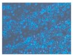
Researchers at the U.S. Department of Energy (DOE)’s Lawrence Berkeley National Laboratory (Berkeley Lab) have successfully grown atomically thin 2D sheets of organic-inorganic hybrid perovskites from solution. The ultrathin sheets are of high quality, large in area, and square-shaped. They also exhibited efficient photoluminescence, color-tunability, and a unique structural relaxation not found in covalent semiconductor sheets.
“We believe this is the first example of 2D atomically thin nanostructures made from ionic materials,” says Peidong Yang, a chemist with Berkeley Lab’s Materials Sciences Division and world authority on nanostructures, who first came up with the idea for this research some 20 years ago. “The results of our study open up opportunities for fundamental research on the synthesis and characterization of atomically thin 2D hybrid perovskites and introduces a new family of 2D solution-processed semiconductors for nanoscale optoelectronic devices, such as field effect transistors and photodetectors.”
Yang, who also holds appointments with the University of California (UC) Berkeley and is a co-director of the Kavli Energy NanoScience Institute (Kavli-ENSI), is the corresponding author of a paper describing this research in the journal Science. The paper is titled “Atomically thin two-dimensional organic-inorganic hybrid perovskites.” The lead authors are Letian Dou, Andrew Wong and Yi Yu, all members of Yang’s research group. Other authors are Minliang Lai, Nikolay Kornienko, Samuel Eaton, Anthony Fu, Connor Bischak, Jie Ma, Tina Ding, Naomi Ginsberg, Lin-Wang Wang and Paul Alivisatos.
Traditional perovskites are typically metal-oxide materials that display a wide range of fascinating electromagnetic properties, including ferroelectricity and piezoelectricity, superconductivity and colossal magnetoresistance. In the past couple of years, organic-inorganic hybrid perovskites have been solution-processed into thin films or bulk crystals for photovoltaic devices that have reached a 20-percent power conversion efficiency. Separating these hybrid materials into individual, free-standing 2D sheets through such techniques as spin-coating, chemical vapor deposition, and mechanical exfoliation has met with limited success.
In 1994, while a PhD student at Harvard University, Yang proposed a method for preparing 2D hybrid perovskite nanostructures and tuning their electronic properties but never acted upon it. This past year, while preparing to move his office, he came upon the proposal and passed it on to co-lead author Dou, a post-doctoral student in his research group. Dou, working mainly with the other lead authors Wong and Yu, used Yang’s proposal to synthesize free-standing 2D sheets of CH3NH3PbI3, a hybrid perovskite made from a blend of lead, bromine, nitrogen, carbon and hydrogen atoms.
“Unlike exfoliation and chemical vapor deposition methods, which normally produce relatively thick perovskite plates, we were able to grow uniform square-shaped 2D crystals on a flat substrate with high yield and excellent reproducibility,” says Dou. “We characterized the structure and composition of individual 2D crystals using a variety of techniques and found they have a slightly shifted band-edge emission that could be attributed to structural relaxation. A preliminary photoluminescence study indicates a band-edge emission at 453 nanometers, which is red-shifted slightly as compared to bulk crystals. This suggests that color-tuning could be achieved in these 2D hybrid perovskites by changing sheet thickness as well as composition via the synthesis of related materials.”
The well-defined geometry of these square-shaped 2D crystals is the mark of high quality crystallinity, and their large size should facilitate their integration into future devices.
“With our technique, vertical and lateral heterostructures can also be achieved,” Yang says. “This opens up new possibilities for the design of materials/devices on an atomic/molecular scale with distinctive new properties.”
Share on:


Suggested Items
Groundbreaking Ceremony Marks the Beginning of a New Era for Newccess Industrial; The Construction of the MINGXIN Building
04/12/2024 | Newccess IndustrialOn a clear and sunny day in March, the groundbreaking ceremony for the MINGXIN Building took place in Shenzhen, China. This moment marked the official commencement of construction for a project that will reshape the semiconductor materials industry.
The Need for a Holistic Global Sustainability Standard
04/10/2024 | Michael Ford, Aegis SoftwareNo one can deny that the resources of our fragile planet are finite. The environment seems like a third party, subject to constant degradation. We’re acutely aware of the effects of pollution on our climate, and despite our “throw-away” culture, recycling and recovery of materials has remained relatively expensive, even as we use more energy just to survive.
iNEMI Publishes Four Roadmap Topics
04/04/2024 | iNEMIThe International Electronics Manufacturing Initiative (iNEMI) announces the availability of the first roadmap topics in the new iNEMI Roadmap format. Printed circuit boards, sustainable electronics, smart manufacturing, and mmWave materials and test are now available online.
Insulectro’s 'Storekeepers' Extend Their Welcome to Technology Village at IPC APEX EXPO
04/03/2024 | InsulectroInsulectro, the largest distributor of materials for use in the manufacture of PCBs and printed electronics, welcomes attendees to its TECHNOLOGY VILLAGE during this year’s IPC APEX EXPO at the Anaheim Convention Center, April 9-11, 2024.
Checking In With ICAPE Group
04/03/2024 | Nolan Johnson, I-Connect007ICAPE Group’s field application engineer Erik Pederson drills down on sustainability, supply chain resiliency, and what value engineering really looks like in this exclusive interview. Founded in 1999, European-based ICAPE Group provides 21 million printed circuit boards and over six million technical parts to manufacturers every month. With 30 PCB manufacturing partners globally and 50 partners providing a wide array of technical parts, ICAPE Group has operations in China, Taiwan, Thailand, South Korea, Vietnam, South Africa, Europe, Mexico, and the United States. The company also focuses on the value proposition for its customers.