


 Designer’s Notebook: What Designers Need to Know About Manufacturing, Part 2
 The Pulse: Drilling Down on Documentation
 Connect the Dots: Designing for Reality: Prioritizing Manufacturability
Jack Pattie Discusses New Ventec Facility
September 30, 2015 | Andy Shaughnessy, PCBDesign007Estimated reading time: Less than a minute
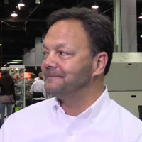
Jack Pattie, CEO of Ventec USA, discusses the company's newest laminate facility, which recently opened in Northern California. He explains how this location, the company's fourth, will help Ventec better serve customers in that region.
To watch this video, click here.
Share on:


Suggested Items
I-Connect007 Editor’s Choice: Five Must-Reads for the Week
04/26/2024 | Andy Shaughnessy, Design007 MagazineIn this week’s roundup, we have a variety of articles covering everything from design through assembly, and even box build. I’ve always wondered whether box build was all it was cracked up to be. Do customers really pick one EMS provider over another because one company offers box build? And if you’ve ever wanted to volunteer, IPC’s Thought Leaders Program is looking for a few good technologists to help them on their mission. Check out Stanton Rak’s article, which was published in the spring issue of IPC Community.
NCAB Group Posts Interim Report Q1 2024
04/26/2024 | NCAB GroupNet sales decreased by 17% to SEK 950.6 million (1,146.4). Compared with the year-earlier period, sales were affected bylower prices and continued inventory adjustments by customers. In USD, net sales decreased 17%. For comparable units, net sales decreased 24% in both SEK and USD.
KYZEN Announces Exclusive Partnership with Manufacturers’ Representative Restronics Florida
04/25/2024 | KYZEN'KYZEN, the global leader in innovative environmentally responsible cleaning chemistries, proudly announces its strategic partnership with Manufacturers’ Representative Restronics Florida. Just like KYZEN’s commitment to continuously improving precision cleaning, Restronics Florida serves as a consultative OEM sales representative organization dedicated to educating customers to enhance their processes and productivity.
Determining the Value-add of Box Build
04/24/2024 | Nolan Johnson, I-Connect007At a strategic level, adding box-building services makes sense for customer loyalty. But is it really that simple? Jon Schmitz, who manages customer engagement at RiverSide Integrated Solutions, talk about about what it really takes to be successful in offering EMS and final assembly services under the same company banner.
Fujitsu, METRON Collaborate to Drive ESG Success
04/24/2024 | JCN NewswireFujitsu Limited and METRON SAS, a French cleantech company specializing in energy management solutions for industrial decarbonization, today announced a strategic initiative to contribute to the realization of carbon neutrality in the manufacturing industry.
Copyright © 2024 I-Connect007 | IPC Publishing Group Inc. All rights reserved.
Log in