


 The Right Approach: I Hear the Train A Comin'
 It’s Only Common Sense: OCCAM—the Time Is Now
 Marcy's Musings: The Growing Industry
New Research Unveils Graphene 'Moth Eyes' to Power Future Smart Technologies
February 29, 2016 | University of SurreyEstimated reading time: 3 minutes
- New ultra-thin, patterned graphene sheets will be essential in designing future technologies such as 'smart wallpaper' and internet-of-things applications
- Advanced Technology Institute uses moth-inspired ultrathin graphene sheets to capture light for use in energy production and to power smart sensors
- Graphene is traditionally an excellent electronic material, but is inefficient for optical applications, absorbs only 2.3% of the light incident on it. A new technique enhances light absorption by 90%.
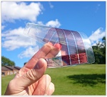
New research published today in Science Advances has shown how graphene can be manipulated to create the most light-absorbent material for its weight, to date. This nanometre-thin material will enable future applications such as 'smart wallpaper' that could generate electricity from waste light or heat, and power a host of applications within the growing 'internet of things'.
Using a technique known as nanotexturing, which involves growing graphene around a textured metallic surface, researchers from the University of Surrey's Advanced Technology Institute took inspiration from nature to create ultra-thin graphene sheets designed to more effectively capture light. Just one atom thick, graphene is very strong but traditionally inefficient at light absorption. To combat this, the team used the nano-patterning to localise light into the narrow spaces between the textured surface, enhancing the amount of light absorbed by the material by about 90%.
"Nature has evolved simple yet powerful adaptations, from which we have taken inspiration in order to answer challenges of future technologies," explained Professor Ravi Silva, Head of the Advanced Technology Institute.
"Moths' eyes have microscopic patterning that allows them to see in the dimmest conditions. These work by channelling light towards the middle of the eye, with the added benefit of eliminating reflections, which would otherwise alert predators of their location. We have used the same technique to make an amazingly thin, efficient, light-absorbent material by patterning graphene in a similar fashion."
Graphene has already been noted for its remarkable electrical conductivity and mechanical strength. Professor Ravi's team understood that for graphene's potential to be realised as material for future applications, it should also harness light and heat effectively.
Professor Silva commented: "Solar cells coated with this material would be able to harvest very dim light. Installed indoors, as part of future 'smart wallpaper' or 'smart windows', this material could generate electricity from waste light or heat, powering a numerous array of smart applications. New types of sensors and energy harvesters connected through the Internet of Things would also benefit from this type of coating."
Dr José Anguita of the University of Surrey and lead author of the paper commented: "As a result of its thinness, graphene is only able to absorb a small percentage of the light that falls on it. For this reason, it is not suitable for the kinds of optoelectronic technologies our 'smart' future will demand."
"Nanotexturing graphene has the effect of channelling the light into the narrow spaces between nanostructures, thereby enhancing the amount of light absorbed by the material. It is now possible to observe strong light absorption from even nanometre-thin films. Typically a graphene sheet would have 2-3% light absorption. Using this method, our ultrathin coating of nanotextured few-layer graphene absorbs 95% of incident light across a broad spectrum, from the UV to the infrared."
Professor Ravi Silva noted: "The next step is to incorporate this material in a variety of existing and emerging technologies. We are very excited about the potential to exploit this material in existing optical devices for performance enhancement, whilst looking towards new applications. Through Surrey's EPSRC funded Graphene Centre, we are looking for industry partners to exploit this technology and are keen to hear from innovative companies who we can explore the future applications of this technology with us."
The Surrey team developed this technology in cooperation with BAE Systems for infrared imaging in opto-MEMs devices.
Share on:


Suggested Items
Warm Windows and Streamlined Skin Patches – IDTechEx Explores Flexible and Printed Electronics
04/26/2024 | IDTechExFlexible and printed electronics can be integrated into cars and homes to create modern aesthetics that are beneficial and easy to use. From luminous car controls to food labels that communicate the quality of food, the uses of this technology are endless and can upgrade many areas of everyday life.
iNEMI Packaging Tech Topic Series: Role of EDA in Advanced Semiconductor Packaging
04/26/2024 | iNEMIAdvanced semiconductor packaging with heterogenous integration has made on-package integration of multiple chips a crucial part of finding alternatives to transistor scaling. Historically, EDA tools for front-end and back-end design have evolved separately; however, design complexity and the increased number of die-to-die or die-to-substrate interconnections has led to the need for EDA tools that can support integration of overall design planning, implementation, and system analysis in a single cockpit.
Koh Young Showcases Award-winning Inspection Solutions at SMTconnect with SmartRep in Hall 4A.225
04/25/2024 | Koh Young TechnologyKoh Young Technology, the industry leader in True 3D measurement-based inspection solutions, will showcase an array of award-winning inspection and measurement solutions at SMTconnect alongside its sales partner, SmartRep, in booth 4A.225 at NürnbergMesse from June 11-13, 2023. The following offers a glimpse into what Koh Young will present at the tradeshow:
Real Time with… IPC APEX EXPO 2024: Plasmatreat: Innovative Surface Preparation Solutions
04/25/2024 | Real Time with...IPC APEX EXPOIn this interview, Editor Nolan Johnson speaks with Hardev Grewal, CEO and president of Plasmatreat, a developer of atmospheric plasma solutions. Plasmatreat uses clean compressed air and electricity to create plasma, offering environmentally friendly methods for surface preparation. Their technology measures plasma density for process optimization and can remove organic micro-contamination. Nolan and Hardev also discuss REDOX-Tool, a new technology for removing metal oxides.
Nanotechnology Market to Surpass $53.51 Billion by 2031
04/25/2024 | PRNewswireSkyQuest projects that the nanotechnology market will attain a value of USD 53.51 billion by 2031, with a CAGR of 36.4% over the forecast period (2024-2031).