


 Happy’s Tech Talk #28: The Power Mesh Architecture for PCBs
 It’s Only Common Sense: Would You Join Your Own Company?
 The Chemical Connection: Reducing Etch System Water Usage, Part 2
Electronics at the Nanoscale
March 26, 2019 | ACN NewswireEstimated reading time: 1 minute
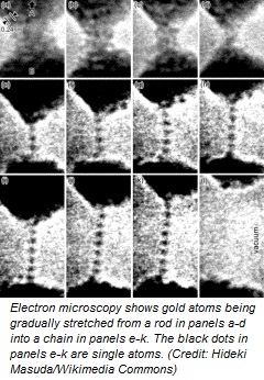
Silver, gold and copper nanowires are leading contenders for next-generation nanoscale devices, however greater understanding of how they work and improved production methods are needed before they can be widely used, explains a recent review in the journal Science and Technology of Advanced Materials.
"Metal nanowires are used for numerous applications, but our understanding of their mechanical properties remains elusive," says Nurul Akmal Che Lah, engineer at Universiti Malaysia Pahang.
Lah and colleague Sonia Trigueros at the University of Oxford reviewed methods for synthesising and analysing silver, gold and copper nanowires for molecular-based electronics.
Molecular electronics uses single molecules, or nanoscale collections of molecules, to create electronic components too small to be seen with the naked eye. For example, molecular wires are one-dimensional chains of single metal atoms which conduct electric current. Molecular electronic devices can be used for a wide range of applications from storage media to catalysts and clinical treatments.
Nanomaterials have different properties from their bulk counterparts. Coinage metals in particular—silver, gold, copper and nickel—have attracted special attention because of their unique physical properties.
Recent advances in experimental techniques have allowed scientists to probe the mechanical properties of nanowires. High precision micromechanical testing devices, such as electron microscopes, scanning force microscopes and X-ray diffraction, can be used to assess crystalline structure, stress-strain relationships, atom-by-atom chemical composition, as well as electronic properties. These methods have revealed that the nanomechanical properties of nanowires are influenced by nanowire structure, surface stress and defect formation.
The researchers investigated recent developments in the synthesis and analysis of metal nanowires. Hydro-solvothermal synthesis, in which metallic structures are grown within a solution, is a relatively simple and inexpensive process. Compared with other methods that require a template or high pressures, hydro-solvothermal synthesis is best suited to industrial application as it doesn't require complex post-processing treatments.
However, synthesis methods must be improved to control the initial size, final size and morphology of the nanowires and produce high yields, whilst also being inexpensive and environmentally friendly. More work needs to be done to further optimise and improve the mechanical properties of coinage nanowires in order to harness their full potential, the researchers conclude.
Share on:


Suggested Items
The Chemical Connection: Reducing Etch System Water Usage, Part 2
05/02/2024 | Don Ball -- Column: The Chemical ConnectionIn my last column, I reviewed some relatively simple ways to reduce water usage in existing etch systems: cutting down cooling coil water flow, adding chillers to replace plant water for cooling, lowering flow rate nozzles for rinses, etc. This month, I’ll continue with more ways to control water usage in your etcher. Most of these are not easily retrofittable to existing equipment but should be given serious consideration when new equipment is contemplated. With the right combination of add-ons, it is possible to bring the amount of water used in an etch system to almost zero.
Designer’s Notebook: What Designers Need to Know About Manufacturing, Part 2
04/24/2024 | Vern Solberg -- Column: Designer's NotebookThe printed circuit board (PCB) is the primary base element for providing the interconnect platform for mounting and electrically joining electronic components. When assessing PCB design complexity, first consider the component area and board area ratio. If the surface area for the component interface is restricted, it may justify adopting multilayer or multilayer sequential buildup (SBU) PCB fabrication to enable a more efficient sub-surface circuit interconnect.
Insulectro’s 'Storekeepers' Extend Their Welcome to Technology Village at IPC APEX EXPO
04/03/2024 | InsulectroInsulectro, the largest distributor of materials for use in the manufacture of PCBs and printed electronics, welcomes attendees to its TECHNOLOGY VILLAGE during this year’s IPC APEX EXPO at the Anaheim Convention Center, April 9-11, 2024.
ENNOVI Introduces a New Flexible Circuit Production Process for Low Voltage Connectivity in EV Battery Cell Contacting Systems
04/03/2024 | PRNewswireENNOVI, a mobility electrification solutions partner, introduces a more advanced and sustainable way of producing flexible circuits for low voltage signals in electric vehicle (EV) battery cell contacting systems.
Heavy Copper PCBs: Bridging the Gap Between Design and Fabrication, Part 1
04/01/2024 | Yash Sutariya, Saturn Electronics ServicesThey call me Sparky. This is due to my talent for getting shocked by a variety of voltages and because I cannot seem to keep my hands out of power control cabinets. While I do not have the time to throw the knife switch to the off position, that doesn’t stop me from sticking screwdrivers into the fuse boxes. In all honesty, I’m lucky to be alive. Fortunately, I also have a talent for building high-voltage heavy copper circuit boards. Since this is where I spend most of my time, I can guide you through some potential design for manufacturability (DFM) hazards you may encounter with heavy copper design.