


 The Government Circuit: Driving Resiliency and Economic Security on Both Sides of the Atlantic
 American Made Advocacy: Taking the Fight to Capitol Hill
 Defense Speak Interpreted: SWaPing Nanosatellites for Defense Systems
BAE Systems Awarded Next Generation Launcher Design Contract
July 7, 2023 | Business WireEstimated reading time: 1 minute
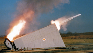
BAE Systems was awarded a $37 million U.S. Department of Defense Ordnance Technology Consortium (DOTC) contract to design the Next Generation Evolved SeaSparrow Missile Launch System (NGELS). The company will support the NATO SeaSparrow Program Office (NSPO) to design and deliver prototype deck launching systems to support the U.S. Navy and allied countries with the Evolved SeaSparrow Missile (ESSM) ship self-defense system.
NGELS is a deck-mounted, fixed-angle launcher that leverages BAE Systems’ Adaptable Deck Launcher (ADL) concept to store and launch ESSMs from Mk 25 missile canisters, which are also produced by BAE Systems. Easily integrated into large deck platforms, NGELS will support the fielding of the latest and most highly-capable ESSM missile, the Block 2 variant, a multi-role surface-to-air and surface-to-surface missile capable of protecting aircraft carriers and other flat-decked ships against advanced air and surface threats. NGELS will use proven Mk 41 Vertical Launching System subsystems to deliver surface-to-air and surface-to-surface defense capabilities to aircraft carriers and amphibious ships in order to defeat missile threats.
“We have a long history of providing missile integration, launching systems, and canister design to the U.S. Navy,” said Brent Butcher, vice president of the weapon systems product line at BAE Systems. “NGELS leverages the expertise of our workforce to provide a ready-to-deploy system that enhances mission effectiveness and enables reliable ship defense for the U.S. Navy. We look forward to working with our customers to bring this enhanced capability to the fleet and introducing it to international users.”
Share on:


Suggested Items
iNEMI Packaging Tech Topic Series: Role of EDA in Advanced Semiconductor Packaging
04/26/2024 | iNEMIAdvanced semiconductor packaging with heterogenous integration has made on-package integration of multiple chips a crucial part of finding alternatives to transistor scaling. Historically, EDA tools for front-end and back-end design have evolved separately; however, design complexity and the increased number of die-to-die or die-to-substrate interconnections has led to the need for EDA tools that can support integration of overall design planning, implementation, and system analysis in a single cockpit.
Cadence, TSMC Collaborate on Wide-Ranging Innovations to Transform System and Semiconductor Design
04/25/2024 | Cadence Design SystemsCadence Design Systems, Inc. and TSMC have extended their longstanding collaboration by announcing a broad range of innovative technology advancements to accelerate design, including developments ranging from 3D-IC and advanced process nodes to design IP and photonics.
Ansys, TSMC Enable a Multiphysics Platform for Optics and Photonics, Addressing Needs of AI, HPC Silicon Systems
04/25/2024 | PRNewswireAnsys announced a collaboration with TSMC on multiphysics software for TSMC's Compact Universal Photonic Engines (COUPE). COUPE is a cutting-edge Silicon Photonics (SiPh) integration system and Co-Packaged Optics platform that mitigates coupling loss while significantly accelerating chip-to-chip and machine-to-machine communication.
Siemens’ Breakthrough Veloce CS Transforms Emulation and Prototyping with Three Novel Products
04/24/2024 | Siemens Digital Industries SoftwareSiemens Digital Industries Software launched the Veloce™ CS hardware-assisted verification and validation system. In a first for the EDA (Electronic Design Automation) industry, Veloce CS incorporates hardware emulation, enterprise prototyping and software prototyping and is built on two highly advanced integrated circuits (ICs) – Siemens’ new, purpose-built Crystal accelerator chip for emulation and the AMD Versal™ Premium VP1902 FPGA adaptive SoC (System-on-a-chip) for enterprise and software prototyping.
Listen Up! The Intricacies of PCB Drilling Detailed in New Podcast Episode
04/25/2024 | I-Connect007In episode 5 of the podcast series, On the Line With: Designing for Reality, Nolan Johnson and Matt Stevenson continue down the manufacturing process, this time focusing on the post-lamination drilling process for PCBs. Matt and Nolan delve into the intricacies of the PCB drilling process, highlighting the importance of hole quality, drill parameters, and design optimization to ensure smooth manufacturing. The conversation covers topics such as drill bit sizes, aspect ratios, vias, challenges in drilling, and ways to enhance efficiency in the drilling department.