


 The Government Circuit: Driving Resiliency and Economic Security on Both Sides of the Atlantic
 American Made Advocacy: Taking the Fight to Capitol Hill
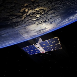
 Defense Speak Interpreted: SWaPing Nanosatellites for Defense Systems
New Flexible Semiconductor for Electronics, Solar Technology and Photo Catalysis
September 13, 2016 | TECHNICAL UNIVERSITY OF MUNICH (TUM)Estimated reading time: 3 minutes
It is the double helix, with its stable and flexible structure of genetic information, that made life on Earth possible in the first place. Now a team from the Technical University of Munich (TUM) has discovered a double helix structure in an inorganic material. The material comprising tin, iodine and phosphorus is a semiconductor with extraordinary optical and electronic properties, as well as extreme mechanical flexibility.
Flexible yet robust - this is one reason why nature codes genetic information in the form of a double helix. Scientists at TU Munich have now discovered an inorganic substance whose elements are arranged in the form of a double helix.
The substance called SnIP, comprising the elements tin (Sn), iodine (I) and phosphorus (P), is a semiconductor. However, unlike conventional inorganic semiconducting materials, it is highly flexible. The centimeter-long fibers can be arbitrarily bent without breaking.
"This property of SnIP is clearly attributable to the double helix," says Daniela Pfister, who discovered the material and works as a researcher in the work group of Tom Nilges, Professor for Synthesis and Characterization of Innovative Materials at TU Munich. "SnIP can be easily produced on a gram scale and is, unlike gallium arsenide, which has similar electronic characteristics, far less toxic."
Countless application possibilities
The semiconducting properties of SnIP promise a wide range of application opportunities, from energy conversion in solar cells and thermoelectric elements to photocatalysts, sensors and optoelectronic elements. By doping with other elements, the electronic characteristics of the new material can be adapted to a wide range of applications.
Due to the arrangement of atoms in the form of a double helix, the fibers, which are up to a centimeter in length can be easily split into thinner strands. The thinnest fibers to date comprise only five double helix strands and are only a few nanometers thick. That opens the door also to nanoelectronic applications.
"Especially the combination of interesting semiconductor properties and mechanical flexibility gives us great optimism regarding possible applications," says Professor Nilges. "Compared to organic solar cells, we hope to achieve significantly higher stability from the inorganic materials. For example, SnIP remains stable up to around 500°C (930 °F)."
Just at the beginning
"Similar to carbon, where we have the three-dimensional (3D) diamond, the two dimensional graphene and the one dimensional nanotubes," explains Professor Nilges, "we here have, alongside the 3D semiconducting material silicon and the 2D material phosphorene, for the first time a one dimensional material - with perspectives that are every bit as exciting as carbon nanotubes."
Just as with carbon nanotubes and polymer-based printing inks, SnIP double helices can be suspended in solvents like toluene. In this way, thin layers can be produced easily and cost-effectively. "But we are only at the very beginning of the materials development stage," says Daniela Pfister. "Every single process step still needs to be worked out."
Since the double helix strands of SnIP come in left and right-handed variants, materials that comprise only one of the two should display special optical characteristics. This makes them highly interesting for optoelectronics applications. But, so far there is no technology available for separating the two variants.
Theoretical calculations by the researchers have shown that a whole range of further elements should form these kinds of inorganic double helices. Extensive patent protection is pending. The researchers are now working intensively on finding suitable production processes for further materials.
Interdisciplinary cooperation
An extensive interdisciplinary alliance is working on the characterization of the new material: Photoluminescence and conductivity measurements have been carried out at the Walter Schottky Institute of the TU Munich. Theoretical chemists from the University of Augsburg collaborated on the theoretical calculations. Researchers from the University of Kiel and the Max Planck Institute of Solid State Research in Stuttgart performed transmission electron microscope investigations. Mössbauer spectra and magnetic properties were measured at the University of Augsburg, while researchers of TU Cottbus contributed thermodynamics measurements.
Share on:


Suggested Items
Material Insight: The Dielectric Constant of PCB Materials
05/17/2024 | Dr. Preeya Kuray -- Column: Material InsightIn the world of PCB design, miniaturization can be achieved by using low dielectric constant (Dk) materials. Low Dk materials can allow for a reduction in thickness while maintaining a given trace width, leading to lower transmission loss and higher density circuitry.
IPC APEX EXPO: Some Thoughts About Growth
05/16/2024 | Dan Feinberg, I-Connect007After two and a half days of wandering the aisles at IPC APEX EXPO 2024, for the first time, I almost felt like I was exploring CES. There were so many booths and exhibits that I could describe, but I’d like to focus on the growth and huge value of this event, which has expanded well beyond just the growing and impressive exhibit show floor.
The Shaughnessy Report: Unlock Your High-speed Material Constraints
05/15/2024 | Andy Shaughnessy -- Column: The Shaughnessy ReportThe world of PCB materials used to be a fairly simple one. It was divided into two groups: the “traditional” laminates, often called FR-4, and the high-speed laminates developed especially for high-speed PCBs. These were two worlds that usually didn’t collide. But then traditional laminates started getting better, and high-speed designers and design engineers took notice and started to reconsider what FR-4 could be used for.
Breaking High-speed Material Constraints: Design007 Magazine — May 2024
05/14/2024 | I-Connect007 Editorial TeamDo you need specialty materials for your high-speed designs? Maybe not. Improvements in resins mean designers of high-speed boards can sometimes use traditional laminate systems instead of high-speed materials, saving time and money while streamlining the fab process. In the May 2024 issue of Design007 Magazine, our contributors explain how to avoid overconstraining your materials when working with high-speed boards.
Indium Experts to Present at Electronics in Harsh Environments SMTA Conference
05/13/2024 | Indium Corporationndium Corporation Technical Manager for Europe, Africa, and the Middle East, Karthik Vijay, will deliver a technical presentation and Indium Corporation Senior Technologist, Dr. Ronald Lasky, will deliver both a workshop and technical presentation at the Electronics in Harsh Environments SMTA Conference on May 14-16 in Copenhagen, Denmark.