


 Marcy's Musings: The Growing Industry
 It’s Only Common Sense: Here’s What To Do After IPC APEX EXPO 2024
 Dan’s Biz Bookshelf: Seeing the How
NIST Researchers Boost Intensity of Nanowire LEDs
March 21, 2019 | NISTEstimated reading time: 2 minutes
Nanowire gurus at the National Institute of Standards and Technology (NIST) have made ultraviolet light-emitting diodes (LEDs) that, thanks to a special type of shell, produce five times higher light intensity than do comparable LEDs based on a simpler shell design.
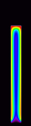
Image Caption: Model of nanowire-based light-emitting diode showing that adding a bit of aluminum to the shell layer (black) directs all recombination of electrons and holes (spaces for electrons) into the nanowire core (multicolored region), producing intense light.
Ultraviolet LEDs are used in a growing number of applications such as polymer curing, water purification and medical disinfection. Micro-LEDs are also of interest for visual displays. NIST staff are experimenting with nanowire-based LEDs for scanning-probe tips intended for electronics and biology applications.
The new, brighter LEDs are an outcome of NIST’s expertise in making high-quality gallium nitride (GaN) nanowires. Lately, researchers have been experimenting with nanowire cores made of silicon-doped GaN, which has extra electrons, surrounded by shells made of magnesium-doped GaN, which has a surplus of “holes” for missing electrons. When an electron and a hole combine, energy is released as light, a process known as electroluminescence.
The NIST group previously demonstrated GaN LEDs that produced light attributed to electrons injected into the shell layer to recombine with holes. The new LEDs have a tiny bit of aluminum added to the shell layer, which reduces losses from electron overflow and light reabsorption.
As described in the journal Nanotechnology, the brighter LEDs are fabricated from nanowires with a so-called “p-i-n” structure, a tri-layer design that injects electrons and holes into the nanowire. The addition of aluminum to the shell helps confine electrons to the nanowire core, boosting the electroluminescence fivefold.
“The role of the aluminum is to introduce an asymmetry in the electrical current that prevents electrons from flowing into the shell layer, which would reduce efficiency, and instead confines electrons and holes to the nanowire core,” first author Matt Brubaker said.
The nanowire test structures were about 440 nanometers (nm) long with a shell thickness of about 40 nm. The final LEDs, including the shells, were almost 10 times larger. Researchers found that the amount of aluminum incorporated into fabricated structures depends on nanowire diameter.
Group leader Kris Bertness said at least two companies are developing micro-LEDs based on nanowires, and NIST has a Cooperative Research and Development Agreement with one of them to develop dopant and structural characterization methods. The researchers have had preliminary discussions with scanning-probe companies about using NIST LEDs in their probe tips, and NIST plans to demonstrate prototype LED tools soon.
The NIST team holds U.S. Patent 8,484,756 on an instrument that combines microwave scanning probe microscopy with an LED for nondestructive, contactless testing of material quality for important semiconductor nanostructures such as transistor channels and individual grains in solar cells. The probe could also be used for biological research on protein unfolding and cell structure.
Share on:


Suggested Items
Happy’s Tech Talk #27: Integrated Mesh Power System (IMPS) for PCBs
04/08/2024 | Happy Holden -- Column: Happy’s Tech TalkA significant decrease in HDI substrate production cost can be achieved by reducing the number of substrate layers from conventional through-hole multilayers and microvia multilayers of eight, 10, 12, and more to only two layers. Besides reducing direct processing steps, the yield will increase as defect-producing operations are eliminated. The integrated mesh power system (IMPS) was invented in the latter years of MCM-D use for thin-film fabrication. Those geometries fit today into our use of ultra HDI.
Insulectro’s 'Storekeepers' Extend Their Welcome to Technology Village at IPC APEX EXPO
04/03/2024 | InsulectroInsulectro, the largest distributor of materials for use in the manufacture of PCBs and printed electronics, welcomes attendees to its TECHNOLOGY VILLAGE during this year’s IPC APEX EXPO at the Anaheim Convention Center, April 9-11, 2024.
Now Available: Episode 4, Season 2 of Designing for Reality—Lamination
04/04/2024 | I-Connect007I-Connect007 has just released the latest episode of its podcast series, On the Line With..., which focuses on designing for reality in the electronics industry. Multilayer boards bring along a completely different set of processes. In this installment, ASC Sunstone VP/Manager Matt Stevenson discusses manufacturing techniques for multilayer boards. Of course, this necessitates a review of drill and registration techniques, followed by the ins and outs of lamination.
Heavy Copper PCBs: Bridging the Gap Between Design and Fabrication, Part 1
04/01/2024 | Yash Sutariya, Saturn Electronics ServicesThey call me Sparky. This is due to my talent for getting shocked by a variety of voltages and because I cannot seem to keep my hands out of power control cabinets. While I do not have the time to throw the knife switch to the off position, that doesn’t stop me from sticking screwdrivers into the fuse boxes. In all honesty, I’m lucky to be alive. Fortunately, I also have a talent for building high-voltage heavy copper circuit boards. Since this is where I spend most of my time, I can guide you through some potential design for manufacturability (DFM) hazards you may encounter with heavy copper design.
Kioxia, WD Elevate Capacity Utilization, Pushing NAND Flash Supply Growth to 10.9%
03/19/2024 | TrendForceTrendForce reports that anticipation of NAND Flash price hikes into Q2 has motivated certain suppliers to minimize losses and lower costs in hopes of returning to profitability this year.