


 Marcy's Musings: The Growing Industry
 It’s Only Common Sense: Here’s What To Do After IPC APEX EXPO 2024
 Dan’s Biz Bookshelf: Seeing the How
Compound Photonics Backplane Enables World’s Smallest MicroLED AR Displays
May 5, 2020 | Business WireEstimated reading time: 2 minutes
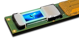
Compound Photonics US Corporation (CP), a global leader providing compact high-resolution microdisplay solutions for Augmented and Mixed Reality (AR/MR), announces today the wide availability of its high-performance digital backplane to leading microLED developers worldwide for integration into complete microdisplay subsystems.
CP re-engineered its market-ready LCoS backplane technology into an innovative constant current drive configuration for microLED pixels based on its industry-leading 0.26” diagonal (~3 ?m pixel) 1080p display format. microLED developers can accelerate their time to market by bonding their devices to a backplane driven by CP’s field-proven NOVA display drive architecture to enable complete display subsystems meeting critical AR requirements for compactness, optical performance and brightness with high frame rate, low latency and low power consumption.
“Our custom, constant current pixel circuit design provides greater tolerance to forward voltage variation and IR drops in the microLED array resulting in a previously unattainable level of uniformity. It additionally features globally on-the-fly programmable pixel current control that greatly increases the system bandwidth, enabling higher frame rates while maintaining full bit depth,” commented Ian Kyles, CP Vice President of Electrical/Software Engineering. “The backplane also has additional steering pixels beyond its native 2048x1080 resolution to enhance alignment/integration of the display within the optical system.”
MicroLED developers using this backplane can access CP’s monolithic integrated display module (IDM) (7.25 x 15.5 x 3.1 mm) with a low pin count interconnect and a direct MIPI input packaged into a compact subsystem amenable to smaller optical engine size. The IDM integrates CP’s proprietary NOVA drive architecture’s software defined platform to enable customizable frame-by-frame control of video frame rates (up to 240 Hz), bit depth, and other parameters to optimize for low latency, short persistence and low power while maintaining near 100% duty cycle according to type of image content and use case.
Andrew Shih, CP’s Marketing and Business Development Manager continued, “Process integration compatibility is also important, as bonding of the microLED array to the backplane requires a highly planar interface. CP’s backplane wafers feature excellent planarity, a direct benefit from extensive process tuning work to meet earlier LCoS requirements. By partnering with CP, whose backplane technology facilitates both wafer level process integration and a direct path to a complete NOVA-based microdisplay subsystem solution, microLED developers can focus on their core competencies in compound semiconductor photonic device engineering and process development while reducing development time and cost.”
A provisional backplane reference specification is presently available for customer review and CP is currently accepting engagements with leading microLED developers.
Share on:


Suggested Items
Intel Brings AI-Platform Innovation to Life at the Olympic Games
04/18/2024 | BUSINESS WIREIntel announced its plans for the Olympic and Paralympic Games Paris 2024. Bringing AI Everywhere, Intel will implement artificial intelligence technology powered by Intel processors on the world’s biggest stage.
The Connection Between Wire Harness and Box Build
04/17/2024 | Nolan Johnson, I-Connect007Christina Rutherford is a technical lead and expert in materials engineering at Honeywell, where her specialty is the design, specification, and manufacture of cables and wire harnesses. Rutherford also sits on the committee for IPC/WHMA-A-620. In this conversation, we explore the changing dynamics in wire harnesses and how they relate to box build. Christina’s standards work allows her to draw insightful parallels between wire harness and box build.
Real Time with... IPC APEX EXPO 2024: Innovations in Thermal, Warpage, and Strain Metrology
04/17/2024 | Real Time with...IPC APEX EXPOEditor Nolan Johnson talks with Neil Hubble, president of Akrometrix, about the company's leadership in thermal, warpage, and strain metrology. Neil details how Akrometrix is committed to addressing customer challenges through technological evolution, innovative solutions, and a focus on data processing. A tabletop unit for thermal warpage testing is showcased at IPC APEX EXPO this year.
Hentec/RPS Publishes an Essential Guide to Selective Soldering Processing Tech Paper
04/17/2024 | Hentec Industries/RPS AutomationHentec Industries/RPS Automation, a leading manufacturer of selective soldering, lead tinning and solderability test equipment, announces that it has published a technical paper describing the critical process parameters that need to be optimized to ensure optimal results and guarantee the utmost in end-product quality.
Connect the Dots: Designing for Reality: Prioritizing Manufacturability
04/11/2024 | Matt Stevenson -- Column: Connect the DotsRealistic PCB designs should prioritize manufacturability and reliability of the PCB as well as meet the other design requirements. To do so, one must account for the production variables associated with individual manufacturing partners. Understanding and creating robust PCB designs, especially in terms of board manufacturing, requires a lot of attention to detail. When more detail is included in the design, the manufacturing process goes more smoothly, and process yields are higher.