


 Flexible Thinking: PCB Designers Still Wanted
 Connect the Dots: Five Best Practices for Designing Flex and Rigid-flex PCBs
 Tim’s Takeaways: Human Ingenuity and the Rigid-flex PCB
MKS Expands Industry Footprint in Asia with Newest HDI PCB Laser Manufacturing Solution
December 10, 2020 | MKS Instruments, Inc.Estimated reading time: 2 minutes
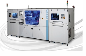
MKS Instruments, Inc., a global provider of technologies that enable advanced processes and improve productivity, announced it has received an order for multiple ESI® Geode™ HDI via drilling systems in Taiwan from a major technology leader in the HDI PCB manufacturing market.
“The market is embracing the economic advantages that the latest MKS developments have to offer,” said John Williams, Vice President and General Manager of MKS’ Equipment and Solutions division. “Our Geode HDI via drilling system meets the needs of high-volume HDI PCB manufacturing, while helping customers secure a technological advantage for current and future product requirements.”
This multi-unit order will support the customer’s existing manufacturing and future technological development through the use of leading-edge via drilling technology. Since its release to the market, the Geode HDI via drilling system has introduced HDI manufacturers to the performance advantages that ESI technology has provided to Flex PCB manufacturers for decades. The Geode platform has seen strong traction amongst the industry’s top players since its recent introduction to the market.
Developed by MKS’ Equipment & Solutions Division, already a market leader in flex PCB laser drilling solutions, the Geode system is optimized to process the rigid HDI PCBs and package substrates widely used in consumer electronics, such as smartphones and other handheld devices. Building on MKS’ technology leadership in laser processing for flexible printed circuits, Geode’s new laser technology and control capabilities deliver breakthrough performance. Its superior throughput, refined power control and small system footprint meet the needs of high-volume PCB manufacturers and technology leaders.
About MKS Instruments
MKS Instruments, Inc. is a global provider of instruments, systems, subsystems and process control solutions that measure, monitor, deliver, analyze, power and control critical parameters of advanced manufacturing processes to improve process performance and productivity for our customers. Our products are derived from our core competencies in pressure measurement and control, flow measurement and control, gas and vapor delivery, gas composition analysis, electronic control technology, reactive gas generation and delivery, power generation and delivery, vacuum technology, lasers, photonics, optics, precision motion control, vibration control and laser-based manufacturing systems solutions. We also provide services relating to the maintenance and repair of our products, installation services and training. Our primary served markets include semiconductor, industrial technologies, life and health sciences, research and defense. Additional information can be found at www.mksinst.com.
About the ESI Brand
ESI® is a brand within the MKS Instruments Equipment & Solutions Division. The ESI portfolio consists of laser-based micro manufacturing systems and component test systems that are used worldwide by manufacturers in the electronics industry to process the materials and components that are an integral part of the electronic devices and systems in use today. Leveraging over 40 years of laser-material interaction expertise and applied laser technology, ESI solutions enable customers to optimize production by providing more control, greater application flexibility and more precise processing of a wide range of materials. The result is higher production quality, increased throughput and higher back-end yields at a lower total cost-of-ownership. Additional information can be found at www.esi.com.
Share on:


Suggested Items
TTM Celebrates the Grand Opening of Its First Manufacturing Facility in Penang
04/25/2024 | TTM Technologies, Inc.TTM Technologies, Inc., a leading global manufacturer of technology solutions including mission systems, radio frequency (RF) components and RF microwave/microelectronic assemblies, and quick-turn and technologically advanced printed circuit boards (PCBs), officially opened its first manufacturing plant in Penang, Malaysia with an investment of USD200 million (approximately RM958 million).
Listen Up! The Intricacies of PCB Drilling Detailed in New Podcast Episode
04/25/2024 | I-Connect007In episode 5 of the podcast series, On the Line With: Designing for Reality, Nolan Johnson and Matt Stevenson continue down the manufacturing process, this time focusing on the post-lamination drilling process for PCBs. Matt and Nolan delve into the intricacies of the PCB drilling process, highlighting the importance of hole quality, drill parameters, and design optimization to ensure smooth manufacturing. The conversation covers topics such as drill bit sizes, aspect ratios, vias, challenges in drilling, and ways to enhance efficiency in the drilling department.
Elevating PCB Design Engineering With IPC Programs
04/24/2024 | Cory Blaylock, IPCIn a monumental stride for the electronics manufacturing industry, IPC has successfully championed the recognition of the PCB Design Engineer as an official occupation by the U.S. Department of Labor (DOL). This pivotal achievement not only underscores the critical role of PCB design engineers within the technology landscape, but also marks the beginning of a transformative journey toward nurturing a robust, skilled workforce ready to propel our industry into the future.
Fujitsu, METRON Collaborate to Drive ESG Success
04/24/2024 | JCN NewswireFujitsu Limited and METRON SAS, a French cleantech company specializing in energy management solutions for industrial decarbonization, today announced a strategic initiative to contribute to the realization of carbon neutrality in the manufacturing industry.
Real Time with... IPC APEX EXPO 2024: Final Finishes and IC Substrate Manufacturing
04/24/2024 | Real Time with...IPC APEX EXPOEditor Marcy LaRont and Richard DePoto, Uyemura's Business Development Manager, engage in a comprehensive discussion about the positive aspects of the show, the benefits of RAIG in final finishes, and the hurdles faced when upgrading your surface finish. Also discussed are the role of Uyemura's MEC pretreatment agents in IC substrate manufacturing and the importance of collaboration and knowledge sharing.