


 The Government Circuit: Driving Resiliency and Economic Security on Both Sides of the Atlantic
 American Made Advocacy: Taking the Fight to Capitol Hill
 Defense Speak Interpreted: SWaPing Nanosatellites for Defense Systems
Nano Dimension’s AME Monolithic RF Communications Circuit Has Been Sent to ISS Flight Studies
March 18, 2021 | Nano DimensionEstimated reading time: 3 minutes
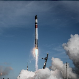
Nano Dimension Ltd., an industry leading Additively Manufactured Electronics (AME)/PE (Printed Electronics) provider, announced today that the first ever integrated RF circuit fabricated by Nano Dimension and designed and integrated by L3Harris, has been flown to the International Space Station (ISS). This project, two years in the making, was selected by the ISS U.S. National Laboratory for space effects studies. The project will provide a systematic analysis of an additively manufactured single board for radio frequency (RF) space systems, especially for nanosatellites, and will communicate with a ground-based satellite tracking system at Embry Riddle Aeronautical University, Daytona Beach, Florida. The primary purpose of the project is to demonstrate the viability of using new technologies, such as multi-level/multi-material AMEs, which use 3D inkjet printer-based technologies to produce monolithic RF communication systems for use in space.
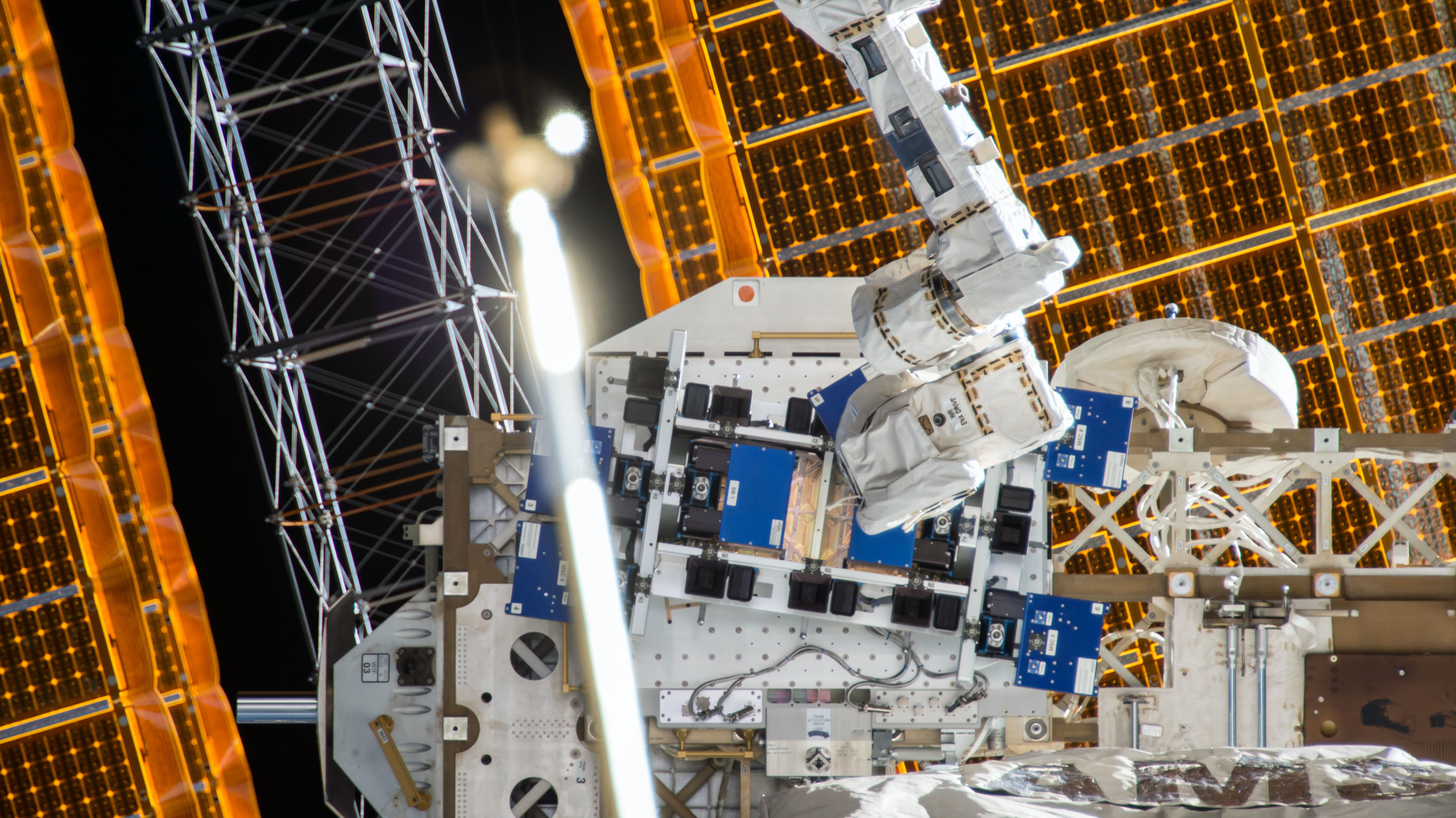
This project, part of the MISSE Flight Facility, is the first systematic experiment by L3Harris and Nano Dimension aiming to analyze the RF properties of additively manufactured High-Performance Electronic Devices (Hi-PEDs™) in a space environment.
L3Harris is a leader in the development of RF circuits for satellites and communications systems. In recent years, research to develop these circuits and systems used for conveying information such as data, video, and voice across long distances has focused on improving mobility and performance.
Nano Dimension fabricated the single RF board using its proprietary additively manufactured electronics process in the DragonFly LDM® system. The board includes the antenna, the electronic traces for mounting all the functional components, and the signal ground plane. The fabricated communications device was designed by L3Harris to operate at 2.4Ghz and to be integrated into the MISSE module and launch. This device will be tested at three program points: pre-flight, in-flight, and post-flight. In this first-of-its-kind space flight experiment, the hardware will fly in the low Earth orbit (LEO) environment for six months on the ISS, which will provide scientists with a better understanding of how AME technology endures in various space environments. Low Earth orbit, a region some 1,200 miles (2,000 km) above the planet, is home to the ISS, as well as a large number of communications satellites, all of which utilize RF communications systems. The possibility of using AME technology for these RF systems had arisen in the past, as it offers several advantages, including the ability to produce low weight, high performance electronic devices, rapid development time, and the ability to fabricate complex shapes and systems that traditional manufacturing cannot.
Dr. Arthur Paolella, senior scientist for the Space and Airborne Systems segment of L3Harris, commented, “Additive manufacturing, or 3D printing, is playing a critical role in advancing the development and applications of small and nano satellites and the overall LEO economy. The applications of 3D printing are broad, touching almost every aspect of research, design, and manufacturing. The major objective of this project is to fly an experiment consisting of an integrated communications circuit fabricated by additive manufacturing and analyze the RF properties of those materials in a space environment. The communications system now on the ISS went through extensive testing in order to prepare it for the mission. Nano Dimension’s contribution to this project was extremely important, as their additively manufactured capability is technologically advanced and superior to existing technologies.”
“This project has been a significant opportunity to qualify our additive manufacturing technology for space applications by fabricating a fully integrated communications board enabled by the multi -material and multi-layer technology of our DragonFly LDM® system,” said Dr. Jaim Nulman, Nano Dimension’s Chief Technology Officer. “The collaboration with L3Harris has increased the technological readiness of our system towards the TR-9 level, which is the highest technology readiness level that indicates the capability for volume deployment in a LEO environment,” added Dr. Nulman.
Share on:


Suggested Items
TTM Celebrates the Grand Opening of Its First Manufacturing Facility in Penang
04/25/2024 | TTM Technologies, Inc.TTM Technologies, Inc., a leading global manufacturer of technology solutions including mission systems, radio frequency (RF) components and RF microwave/microelectronic assemblies, and quick-turn and technologically advanced printed circuit boards (PCBs), officially opened its first manufacturing plant in Penang, Malaysia with an investment of USD200 million (approximately RM958 million).
Elevating PCB Design Engineering With IPC Programs
04/24/2024 | Cory Blaylock, IPCIn a monumental stride for the electronics manufacturing industry, IPC has successfully championed the recognition of the PCB Design Engineer as an official occupation by the U.S. Department of Labor (DOL). This pivotal achievement not only underscores the critical role of PCB design engineers within the technology landscape, but also marks the beginning of a transformative journey toward nurturing a robust, skilled workforce ready to propel our industry into the future.
Fujitsu, METRON Collaborate to Drive ESG Success
04/24/2024 | JCN NewswireFujitsu Limited and METRON SAS, a French cleantech company specializing in energy management solutions for industrial decarbonization, today announced a strategic initiative to contribute to the realization of carbon neutrality in the manufacturing industry.
Real Time with... IPC APEX EXPO 2024: Final Finishes and IC Substrate Manufacturing
04/24/2024 | Real Time with...IPC APEX EXPOEditor Marcy LaRont and Richard DePoto, Uyemura's Business Development Manager, engage in a comprehensive discussion about the positive aspects of the show, the benefits of RAIG in final finishes, and the hurdles faced when upgrading your surface finish. Also discussed are the role of Uyemura's MEC pretreatment agents in IC substrate manufacturing and the importance of collaboration and knowledge sharing.
Women MAKE Awards Recognizes GlobalFoundries’ Jennifer Robbins and Katelyn Harrison for Manufacturing Excellence
04/24/2024 | GlobalFoundriesThe Manufacturing Institute (MI)—the workforce development and education affiliate of the National Association of Manufacturers—honored two outstanding women from GlobalFoundries (GF) at their annual Women MAKE Awards. Jennifer (Jenny) Robbins, Senior Director, Central Facilities, was recognized as a 2024 Women MAKE Awards Honoree, while Katelyn Harrison, Senior Integration Engineer, was honored as an Emerging Leader.