


 The Right Approach: I Hear the Train A Comin'
 It’s Only Common Sense: OCCAM—the Time Is Now
 Marcy's Musings: The Growing Industry
The Cool Solution to Electronics Heat Dissipation
June 11, 2015 | SLAC National Accelerator LaboratoryEstimated reading time: 3 minutes
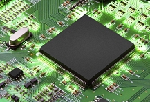
The heat that builds up in the shuttling of current in electronics is an important obstacle to packing more computing power into ever-smaller devices: Excess heat can cause them to fail or sap their efficiency.
Now, X-ray studies at the Department of Energy’s SLAC National Accelerator Laboratory have for the first time observed an exotic property that could warp the electronic structure of a material in a way that reduces heat buildup and improves performance in ever-smaller computer components.
The research was conducted, in part, at SLAC’s Stanford Synchrotron Radiation Lightsource (SSRL), a DOE Office of Science User Facility, and published this month in the print edition of Nature Materials.
Energy-bending Properties
The team studied a form of iridium oxide, Sr3Ir2O7, that belongs to a class of so-called correlated materials in which electrons can be made to behave in sync. It is a candidate for reducing the heat generated by the billions of transistors at the core of modern computers.
The researchers discovered that the material has a long-theorized property, formerly found only in 2-D materials and known as 3-D negative electronic compressibility, that is caused by its unusual electronic structure.
The electronic structure of a material is typically rigid, with distinct energy levels or “bands” that fill up as electrons are added. These levels are determined by the atomic structure and chemical composition of the material. In the study, these energy levels were observed to deform drastically, in a fluid way, as more electrons poured in, while the physical structure of the material did not change in any significant way.
“Imagine pouring water into a cup and watching the water level in the cup appear to dip as the cup deforms,” said Junfeng He, a Boston College researcher who led the study. “That’s how 3-D negative electronic compressibility appears to operate.” But in this case, it is the material’s electronic structure – which defines how it can store or flow electric current – rather than its physical structure that substantially warps as electrons are added.
Guided by theoretical calculations led by Arun Bansil, a professor of physics at Northeastern University, researchers found that a gap between different groupings of energy bands in the sample material actually shrank as electrons were added, reducing the material’s stored energy level – like the water level appearing to decline in the cup example.
In principle, using metal electrodes that have this property in the microscopic gates that regulate the flow of electrons in transistors could substantially enhance their efficiency and reduce heat buildup, said He, who will soon join SLAC as a postdoctoral researcher.
Building a Better Transistor
Rui-Hua He, an assistant professor of physics at Boston College who is a spokesperson for the research, said, “Replacing normal metals in transistors with materials like this that have negative electronic compressibility presents an intriguing alternative to current approaches, with a goal of continuing device miniaturization.” He added, “We are now working on the first demonstration of their potential application to transistors.”
Researchers employed an advanced X-ray technique at SSRL, set up and maintained by SLAC staff scientists Donghui Lu and Makoto Hashimoto, to precisely measure the electronic structure of the material. The negative electronic compressibility they found shows promise for reducing power requirements needed to move electric current around a semiconductor, for example, which would reduce the heat it generates and make electrical switching more efficient.
Previous studies had observed a 2-D version of negative electronic compressibility in other materials, but researchers said the 3-D form has greater potential for application in semiconductors because it is more compatible with their present-day architecture, can potentially be used at room temperature and can be adapted for different applications by adjusting its thickness.
“This work informs us of the importance to continually look for other new materials with novel physical properties for use in transistors and for other applications,” said Stephen Wilson, an assistant professor of materials at the University of California, Santa Barbara, who prepared the sample materials.
Participating researchers were from Boston College, Northeastern University, SLAC’s SSRL and Stanford Institute for Materials and Energy Sciences (SIMES), Lawrence Berkeley National Laboratory, Peking University in China, Hiroshima Synchrotron Radiation Center in Japan and the University of California, Santa Barbara. The work was supported by Boston College, the U.S. National Science Foundation, the W. M. Keck Foundation and the DOE Office of Basic Energy Sciences.
Share on:


Suggested Items
Real Time with... IPC APEX EXPO 2024: Sustainability in the Industry
04/26/2024 | Real Time with...IPC APEX EXPOGuest Editor Henry Crandall and Chris Nash of Indium Corporation discuss the company's 90th anniversary and its focus on sustainability. They focus on the benefits of sustainable materials, their compatibility, and value propositions. The conversation also highlights how Durafuse LT technology's role in reducing reflow temperatures is leading to significant cost and energy savings. Nash also touches on downstream sustainability efforts such as using recycled materials for packaging.
SMC Korea 2024 to Highlight Semiconductor Materials Trends and Innovations on Industry’s Path to $1 Trillion
04/24/2024 | SEMIWith Korea a major consumer of semiconductor materials and advanced materials a key driver of innovation on the industry’s path to $1 trillion, industry leaders and experts will gather at SMC (Strategic Materials Conference) Korea 2024 on May 29 at the Suwon Convention Center in Gyeonggi-do, South Korea to provide insights into the latest materials developments and trends. Registration is open.
Groundbreaking Ceremony Marks the Beginning of a New Era for Newccess Industrial; The Construction of the MINGXIN Building
04/12/2024 | Newccess IndustrialOn a clear and sunny day in March, the groundbreaking ceremony for the MINGXIN Building took place in Shenzhen, China. This moment marked the official commencement of construction for a project that will reshape the semiconductor materials industry.
The Need for a Holistic Global Sustainability Standard
04/10/2024 | Michael Ford, Aegis SoftwareNo one can deny that the resources of our fragile planet are finite. The environment seems like a third party, subject to constant degradation. We’re acutely aware of the effects of pollution on our climate, and despite our “throw-away” culture, recycling and recovery of materials has remained relatively expensive, even as we use more energy just to survive.
iNEMI Publishes Four Roadmap Topics
04/04/2024 | iNEMIThe International Electronics Manufacturing Initiative (iNEMI) announces the availability of the first roadmap topics in the new iNEMI Roadmap format. Printed circuit boards, sustainable electronics, smart manufacturing, and mmWave materials and test are now available online.