


 The Right Approach: I Hear the Train A Comin'
 It’s Only Common Sense: OCCAM—the Time Is Now
 Marcy's Musings: The Growing Industry
Towards Graphene Biosensors
June 25, 2015 | Helmholtz Zentrum BerlinEstimated reading time: 2 minutes
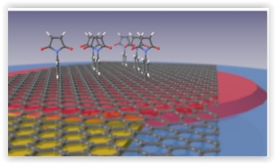
For the first time, a team of scientists has succeeded in precisely measuring and controlling the thickness of an organic compound that has been bound to a graphene layer. This might enable graphene to be used as a sensitive detector for biological molecules in the future.
Pure carbon occurs in many forms. Besides the classical configurations found in diamonds, graphite, and coal, there are other younger exotic cousins such as graphene. Its structure resembles a honeycomb – a hexagonal mesh with a carbon atom at every corner – that is only a single atomic layer thick. Hence, it is essentially two-dimensional. As a result, graphene is extremely conductive, completely transparent, and quite resilient both chemically and mechanically.
Graphene is not very selective
It has long been known that graphene is also fundamentally suited to detecting traces of organic molecules. This is because the electrical conductivity of graphene drops as soon as foreign molecules bind to it. The problem, though, is that this happens with almost every molecule. Graphene is not very selective, which makes it very difficult to differentiate molecules. Therefore, it cannot be used as a sensor.
Now, mounting brackets for detector molecules attached
Now a team from the HZB Institute for Silicon Photovoltaics has found a way to increase the selectivity. They were successful in electrochemically activating graphene and preparing it to host molecules that act as selective binding sites. To accomplish this, para-maleimidophenyl groups from an organic solution were grafted to the surface of the graphene. These organic molecules behave like mounting brackets to which the selective detector molecules can be attached in the next step. “Thanks to these molecules, the graphene can now be employed for detecting various substances similar to how a key fits a lock”, explains Dr. Marc Gluba. The “lock” molecules on the surface are highly selective and only absorb the matching “key” molecules.
Large graphene surfaces at HZB
Other research groups had also carried out experiments along these lines. However, they only had tiny graphene flakes with diameters in the microns available to them, so that edge effects predominated. Meanwhile, physicists and chemists at HZB produced graphene surfaces several square centimeters in size so that edge effects play hardly any role in comparison to the surface processes. Then, they transferred the graphene layer to a quartz crystal microbalance. Any increase in mass alters the oscillatory frequency of the quartz crystal that even small amounts right down to individual molecular layers can be measured.
Precise detection and control
“For the first time, we were able to precisely and accurately detect how many molecules actually were grafted to the surface of the graphene”, reports junior researcher Felix Rösicke, who investigated this problem for his doctoral dissertation. “In addition, we can precisely control how many molecules bind to the graphene by adjusting an applied voltage”, explains Dr. Jörg Rappich from the HZB Institute for Silicon Photovoltaics, Rösicke’s advisor.
“The hopes we have for graphene are really enormous”, says Prof. Norbert Nickel, head of the research team. For example, one thing you could imagine would be a really inexpensive "lab-on-a-chip” – you would apply a single drop of blood and immediately obtain data for important medical diagnostics.
Share on:


Suggested Items
Real Time with… IPC APEX EXPO 2024: Exploring the Future of Surface Finishes
04/25/2024 | Real Time with...IPC APEX EXPOJoe McGurran, product marketing director for MKS Atotech, looks into the future of surface finishes, discussing less nickel, reduced thickness, technologies influencing HDI and UHDI, and the benefits of nickel-free surface finishes. He also touches on popular finishes like ENIG and palladium immersion gold and discusses the value proposition of making a change.
Designer’s Notebook: What Designers Need to Know About Manufacturing, Part 2
04/24/2024 | Vern Solberg -- Column: Designer's NotebookThe printed circuit board (PCB) is the primary base element for providing the interconnect platform for mounting and electrically joining electronic components. When assessing PCB design complexity, first consider the component area and board area ratio. If the surface area for the component interface is restricted, it may justify adopting multilayer or multilayer sequential buildup (SBU) PCB fabrication to enable a more efficient sub-surface circuit interconnect.
IDTechEx Report Unveils 3D Electronics Status and Opportunities
04/22/2024 | PRNewswire3D electronics is an emerging manufacturing approach that enables electronics to be integrated within or onto the surface of objects. 3D electronic manufacturing techniques empower new features, including mass customizability, greater integration, and improved sustainability in the electronics industry.
NASA, Japan Advance Space Cooperation, Sign Agreement for Lunar Rover
04/11/2024 | NASANASA Administrator Bill Nelson and Japan’s Minister of Education, Culture, Sports, Science and Technology (MEXT) Masahito Moriyama have signed an agreement to advance sustainable human exploration of the Moon.
Lockheed Martin Conducts Historic LRASM Flight Test
04/04/2024 | Lockheed MartinThe U.S. Navy in partnership with Lockheed Martin [NYSE: LMT] successfully conducted a historic Long-Range Anti-Ship Missile (LRASM) flight test with four missiles simultaneously in flight.