


 It’s Only Common Sense: OCCAM—the Time Is Now
 Marcy's Musings: The Growing Industry
 Dan’s Biz Bookshelf: Seeing the How
Detecting Spin Precession in Silicon Nanowires
June 25, 2015 | U.S. Naval Research LaboratoryEstimated reading time: 3 minutes
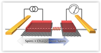
Scientists at the U.S. Naval Research Laboratory (NRL) have reported the first observation of spin precession of spin currents flowing in a silicon nanowire (NW) transport channel, and determined spin lifetimes and corresponding spin diffusion lengths in these nanoscale spintronic devices. The spin currents were electrically injected and detected using ferromagnetic metal contacts with a tunnel barrier consisting of single layer graphene between the metal and silicon NW.
False color atomic force microscopy image of a silicon nanowireFalse color atomic force microscopy image of a silicon nanowire with the four contacts used in the spin measurements. The ferromagnetic metal / graphene tunnel barrier contacts used to inject and detect spin appear as blue, the gold ohmic reference contacts appear as yellow, and the green line is the silicon nanowire transport channel. The bright dot on the end of the nanowire is the gold nanoparticle used to seed the nanowire growth.
The NRL research team observed spin precession (the Hanle effect) for both the spin-polarized charge near the contact interface and for pure spin currents flowing in the NW channel. The latter unambiguously shows that spins have been injected and transported in the Si NW. The use of graphene as the tunnel barrier provides a low-resistance area product contact and clean magnetic switching characteristics, because it smoothly bridges the NW and minimizes complicated magnetic domains that otherwise compromise the magnetic behavior. The team's discovery is an essential step toward the realization of highly scaled semiconductor spintronic devices. The research results are reported in the 19 June 2015 issue of Nature Communications (DOI 10.1038/ncomms8541).
Semiconductor nanowires provide an avenue to further reduce the ever-shrinking dimensions of transistors. Including electron spin as an additional state variable offers new prospects for information processing, enabling future non-volatile, reprogrammable devices beyond the current semiconductor technology roadmap. Silicon is an ideal host for such a spin-based technology because its intrinsic properties promote spin transport, explains principal investigator Dr. Olaf van't Erve.
Realization of spin-based Si NW devices requires efficient electrical spin injection and detection, which depend critically on the interface resistance between a ferromagnetic metal contact and the NW. This is especially problematic with semiconducting NWs because of the exceedingly small contact area, which can be of order 100 nm2. Researchers have shown standard oxide tunnel barriers to provide good spin injection into planar Si structures, but such contacts grown on NWs are often too resistive to yield reliable and consistent results. The NRL team developed and used a graphene tunnel barrier contact that produces excellent spin injection and also satisfies several key technical criteria: it provides a low resistance-area product, a highly uniform tunnel layer with well-controlled thickness, clean magnetic switching characteristics for the magnetic contacts, and compatibility with both the ferromagnetic metal and silicon NW.
Using intrinsic 2D layers such as graphene or hexagonal boron nitride as tunnel contacts on nanowires offers many advantages over conventional materials deposited by vapor deposition (such as Al2O3 or MgO), enabling a path to highly scaled electronic and spintronic devices. The use of multilayer rather than single layer graphene in such structures may provide much higher values of the tunnel spin polarization because of band structure derived spin filtering effects predicted for selected ferromagnetic metal / multi-layer graphene structures. This increase would further improve the performance of nanowire spintronic devices by providing higher signal to noise ratios and corresponding operating speeds, advancing the techological applications of nanowire devices.
The NRL research team includes Dr. Olaf van't Erve, Dr. Adam Friedman, Dr. Connie Li, and Dr. Berend Jonker from the Materials Science and Technology Division, and Dr. Jeremy Robinson from the Electronics Science and Technology Division.
About the U.S. Naval Research Laboratory
The U.S. Naval Research Laboratory is the Navy's full-spectrum corporate laboratory, conducting a broadly based multidisciplinary program of scientific research and advanced technological development. The Laboratory, with a total complement of approximately 2,500 personnel, is located in southwest Washington, D.C., with other major sites at the Stennis Space Center, Miss., and Monterey, Calif. NRL has served the Navy and the nation for over 90 years and continues to meet the complex technological challenges of today's world. For more information, visit the NRL homepage or join the conversation on Twitter, Facebook, and YouTube.
Share on:


Suggested Items
Water Management in a Large Printed Circuit Board Manufacturer
04/15/2024 | Charles Nehrig, TTM TechnologiesTTM’s environmental management is grounded in its Environmental Statement and Environmental Policy, which promote measures that make for a more responsible environmental management process. Our management system helps TTM work toward minimizing its environmental footprint and increasing the sustainability of its operations. TTM monitors its environmental performance just as it monitors its operational performance, and provides the resources required to adhere to the Company’s environmental responsibilities.
Happy’s Tech Talk #27: Integrated Mesh Power System (IMPS) for PCBs
04/08/2024 | Happy Holden -- Column: Happy’s Tech TalkA significant decrease in HDI substrate production cost can be achieved by reducing the number of substrate layers from conventional through-hole multilayers and microvia multilayers of eight, 10, 12, and more to only two layers. Besides reducing direct processing steps, the yield will increase as defect-producing operations are eliminated. The integrated mesh power system (IMPS) was invented in the latter years of MCM-D use for thin-film fabrication. Those geometries fit today into our use of ultra HDI.
Trouble in Your Tank: Supporting IC Substrates and Advanced Packaging, Part 5
03/19/2024 | Michael Carano -- Column: Trouble in Your TankDirect metallization systems based on conductive graphite or carbon dispersion are quickly gaining acceptance worldwide. Indeed, the environmental and productivity gains one can achieve with these processes are outstanding. In today’s highly competitive and litigious environment, direct metallization reduces costs associated with compliance, waste treatment, and legal issues related to chemical exposure. What makes these processes leaders in the direct metallization space?
Indium Corporation Experts to Present at SEMI THERM
03/07/2024 | Indium CorporationIndium Corporation Global Account Manager and Senior Thermal Technologist Tim Jensen and Product Development Specialist for Thermal Interface Materials Miloš Lazić will present on thermal interface material (TIM) technology at SEMI-THERM, taking place March 25–28 in San Jose, California, U.S.
Indium Corporation to Showcase Proven EV Products and High-Reliability Alloys at Productronica China
02/28/2024 | Indium CorporationAs a materials pioneer and trusted partner in electric vehicle (EV) and e-Mobility manufacturing, Indium Corporation is proud to showcase its high-reliability alloys and soldering solutions at Productronica China, March 20-22, in Shanghai.