


 It’s Only Common Sense: OCCAM—the Time Is Now
 Marcy's Musings: The Growing Industry
 Dan’s Biz Bookshelf: Seeing the How
The Iron Stepping Stones To Better Wearable Tech Without Semiconductors
February 5, 2016 | Michigan Technological UniversityEstimated reading time: 3 minutes
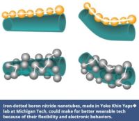
The road to more versatile wearable technology is dotted with iron. Specifically, quantum dots of iron arranged on boron nitride nanotubes (BNNTs). The new material is the subject of a study published in Scientific Reports in February, led by Yoke Khin Yap, a professor of physics at Michigan Technological University.
Yap says the iron-studded BNNTs are pushing the boundaries of electronics hardware. The transistors modulating electron flow need an upgrade.
“Look beyond semiconductors,” he says, explaining that materials like silicon semiconductors tend to overheat, can only get so small and leak electric current. The key to revamping the fundamental base of transistors is creating a series of stepping-stones.
Quantum Dots
The nanotubes are the mainframe of this new material. BNNTs are great insulators and terrible at conducting electricity. While at first that seems like an odd choice for electronics, the insulating effect of BNNTs is crucial to prevent current leakage and overheating. Additionally, electron flow will only occur across the metal dots on the BNNTs.
In past research, Yap and his team used gold for quantum dots, placed along a BNNT in a tidy line. With enough energy potential, the electrons are repelled by the insulating BNNT and hopscotch from gold dot to gold dot. This electron movement is called quantum tunneling.
“Imagine this as a river, and there’s no bridge; it’s too big to hop over,” Yap says. “Now, picture having stepping stones across the river—you can cross over, but only when you have enough energy to do so.”
Nanotech for Wearable Electronics
Unlike with semiconductors, there is no classical resistance with quantum tunneling. No resistance means no heat. Plus, these materials are very small; the nanomaterials enable the transistors to shrink as well. An added bonus is that BNNTs are also quite flexible, a boon for wearable electronics.
“Here’s where the challenge comes in,” Yap says, holding up a pen to demonstrate. He gestures along the length of the pen, which mimics a straight BNNT, tapping out a line of quantum dots. “We have an array here to do quantum tunneling, but what if we want to bend the array to be flexible like a piece of wearable electronics?”
Yap sets down the pen and curls up his index finger: “And if I bend the dots, the distance between them changes—in doing so, we change the electronic behavior.”
Changing the behavior means that the quantum tunneling may not work. The solution is to get out of line: Yap and his team arranged a grid of quantum dots around the outside of the BNNT.
“This time we used iron instead of gold,” Yap adds, explaining that gold’s melting temperature was low for the process his team used. “And when we tested the material, the electrons distributed uniformly across the whole surface of the nanotubes.”
That means that instead of having a line of stepping stones, there are many different paths across the river, and an electron will jump to the nearest one. For future use in wearable electronics, the multiplicity of paths ensures electricity is moving from one riverbank to the next, one way or another. Using scanning tunneling microscopy inside a transmission electron microscope (STM-TEM), the team successfully bent the iron dot-coated BNNT while monitoring the electron flows. The electronic behaviors remain the same even when the BNNT was bent all the way up to 75 degrees.
Next Steps
Yap says that this experiment is a proof of concept. While the iron BNNT material shows promise, it’s not a full transistor yet, capable of modulating electron movement. Right now, it’s called a flexible tunneling channel.
“Next, we’ll put the BNNT and iron onto a bendable plastic substrate,” Yap says. “Then we’ll bend this substrate and watch where the electrons go.”
This experimental work is complemented by computer simulations by John Jaszczak, professor of physics, and Paul Bergstrom, professor of electrical and computer engineering.
Which route the electricity takes is hard to track, which will be the main challenge for the next experiment. But one direction is certain, Yap’s research is headed down a path to change the basic level of electronics and make wearable tech more adaptable.
About Michigan Technological University
Michigan Technological University is a leading public research university developing new technologies and preparing students to create the future for a prosperous and sustainable world. Michigan Tech offers more than 120 undergraduate and graduate degree programs in engineering; forest resources; computing; technology; business; economics; natural, physical and environmental sciences; arts; humanities; and social sciences.
Share on:


Suggested Items
Book Excerpt: The Printed Circuit Assembler’s Guide to... Factory Analytics
04/24/2024 | I-Connect007 Editorial TeamIn our fast-changing, deeply competitive, and margin-tight industry, factory analytics can be the key to unlocking untapped improvements to guarantee a thriving business. On top of that, electronics manufacturers are facing a tremendous burden to do more with less. If you don't already have a copy of this book, what follows is an excerpt from the introduction chapter of 'The Printed Circuit Assembler’s Guide to... Factory Analytics: Unlocking Efficiency Through Data Insights' to whet your appetite.
Listen Up! The Intricacies of PCB Drilling Detailed in New Podcast Episode
04/25/2024 | I-Connect007In episode 5 of the podcast series, On the Line With: Designing for Reality, Nolan Johnson and Matt Stevenson continue down the manufacturing process, this time focusing on the post-lamination drilling process for PCBs. Matt and Nolan delve into the intricacies of the PCB drilling process, highlighting the importance of hole quality, drill parameters, and design optimization to ensure smooth manufacturing. The conversation covers topics such as drill bit sizes, aspect ratios, vias, challenges in drilling, and ways to enhance efficiency in the drilling department.
Elevating PCB Design Engineering With IPC Programs
04/24/2024 | Cory Blaylock, IPCIn a monumental stride for the electronics manufacturing industry, IPC has successfully championed the recognition of the PCB Design Engineer as an official occupation by the U.S. Department of Labor (DOL). This pivotal achievement not only underscores the critical role of PCB design engineers within the technology landscape, but also marks the beginning of a transformative journey toward nurturing a robust, skilled workforce ready to propel our industry into the future.
Winner of The Science Show Rakett 69 Receives Incap Scholarship
04/24/2024 | IncapThe winner of the Rakett 69 science show, Andri Türkson, who stood out as an electronics enthusiast, received a scholarship from Incap Estonia, along with an internship opportunity in Saaremaa.
Alternative Manufacturing Inc. Awarded QML Requalification to IPC J-STD-001 and IPC-A-610
04/24/2024 | IPCIPC's Validation Services Program has awarded an IPC J-STD-001 and IPC-A-610 Qualified Manufacturers Listing (QML) requalification to Alternative Manufacturing Inc (AMI).